Solid photogvapic taking cameva and mfg method thereof

A technology of a solid-state imaging device and a manufacturing method, which is applied in the fields of semiconductor/solid-state device manufacturing, electric solid-state device, image communication, etc., can solve the problem of difficulty in obtaining a solid-state imaging device with high light-gathering ability, etc.

Inactive Publication Date: 2004-03-24
SANYO ELECTRIC CO LTD
View PDF0 Cites 7 Cited by
  • Summary
  • Abstract
  • Description
  • Claims
  • Application Information

AI Technical Summary

Problems solved by technology

As a result, there is a problem that it is difficult to obtain a solid-state imaging device with a high light-gathering ability after the optical lens and the solid-state imaging element are integrated.

Method used


Image

  • Solid photogvapic taking cameva and mfg method thereof
  • Solid photogvapic taking cameva and mfg method thereof
  • Solid photogvapic taking cameva and mfg method thereof

Examples


Embodiment approach 1

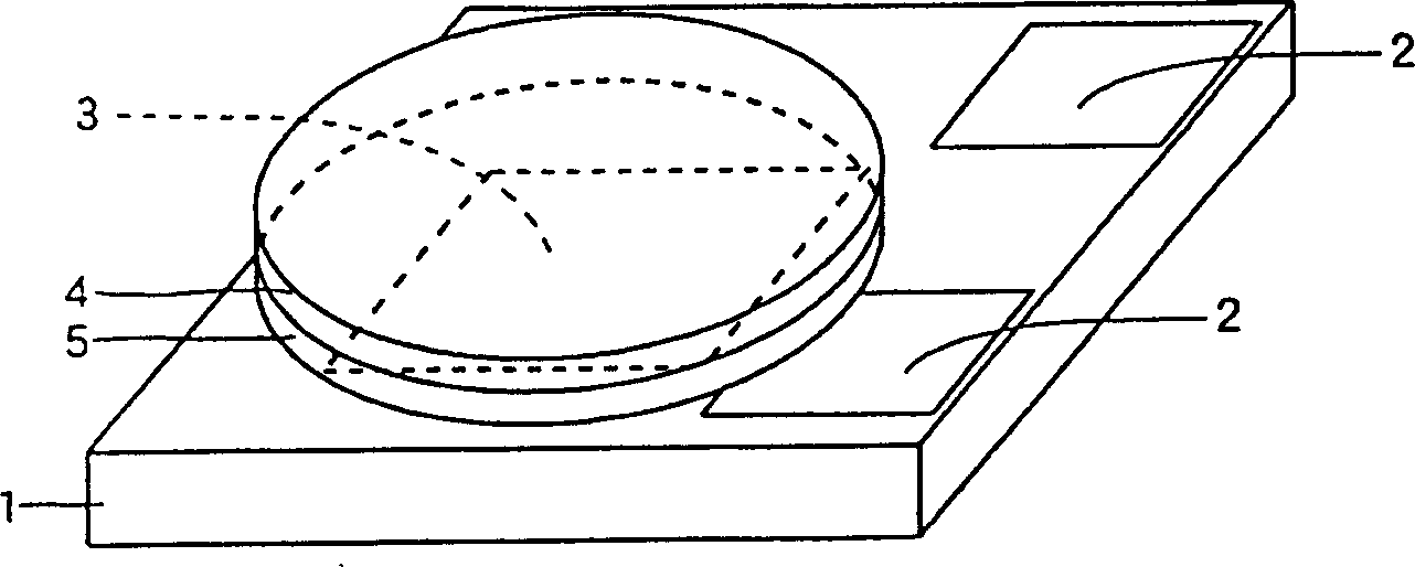
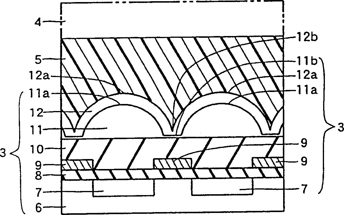
[0048] First, refer to figure 1 and figure 2 , the structure of the solid-state imaging device according to Embodiment 1 will be described.

[0049] Such as figure 1 As shown, in Embodiment 1, peripheral circuits 2 such as drivers and a solid-state imaging device 3 are assembled on a mounting substrate 1 . An optical lens 4 for collecting reflected light from a subject is integrally formed on the solid-state imaging element 3 via a resin layer 5 . The resin layer 5 is formed of epoxy resin with a thickness of about 1 mm to 2 mm, and has a refractive index of about 1.5.

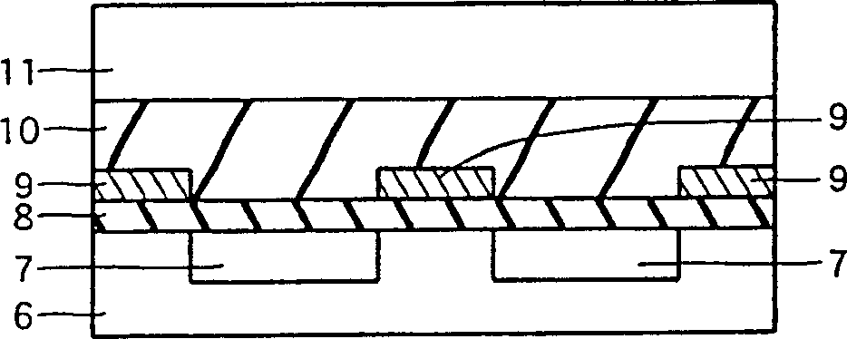
[0050] The specific structure of the solid-state imaging element 3 is as follows: figure 2 As shown, a light receiving portion 7 having a photoelectric conversion function of converting incident light into signal charges is formed on a predetermined region of the Si substrate 6 . On the Si substrate 6 on which the light receiving part 7 is formed 2 Interlayer insulating film 8 is formed to a thicknes...


PUM


Abstract

A solid state image device capable of attaining high condensability also when integrating an optical lens and a solid state image sensor with each other is provided. This solid state image device comprises an optical lens, a solid state image sensor including a microlens, and a resin layer formed between the optical lens and the microlens of the solid state image sensor. Thus, the solid state image device can refract light incident upon the microlens from the resin layer also when the resin layer is formed between the solid state image sensor and the optical lens.

Description

technical field [0001] The present invention relates to a solid-state imaging device and a manufacturing method thereof, and particularly to a solid-state imaging device including a solid-state imaging element having a photoelectric conversion function and a manufacturing method thereof. Background technique [0002] A solid-state imaging device having a solid-state imaging element having a photoelectric conversion function has been around for a long time. Figure 21 This is a schematic diagram showing the overall structure of a conventional solid-state imaging device. Figure 22 yes Figure 21 A cross-sectional view of a solid-state imaging element of a conventional solid-state imaging device is shown. First, refer to Figure 21 and Figure 22 , the structure of a conventional solid-state imaging device will be described. [0003] Conventional solid-state imaging devices such as Figure 21 As shown, above the solid-state imaging element 103, an optical lens 104 for collec...

Claims


Application Information

Patent Timeline
Patent Type & Authority Applications(China)
IPC IPC(8): G02B3/00H01L21/00H01L27/14H04N5/335H04N5/369
CPCH01L27/1462H01L27/14685H01L27/14625H01L27/14627H01L27/14623
Inventor 泉诚冲川满笹田一弘松原直辉小出辰彦
Owner SANYO ELECTRIC CO LTD
Why Eureka
Try Eureka