

Light-emitting diode structure
A technology of light-emitting diodes and boron phosphide, applied in lasers, semiconductor devices, phonon exciters, etc., can solve problems such as high manufacturing costs, difficult manufacturing processes, and poor luminous efficiency of components
- Summary
- Abstract
- Description
- Claims
- Application Information
AI Technical Summary
Problems solved by technology
Method used
Image

Examples
Embodiment 1
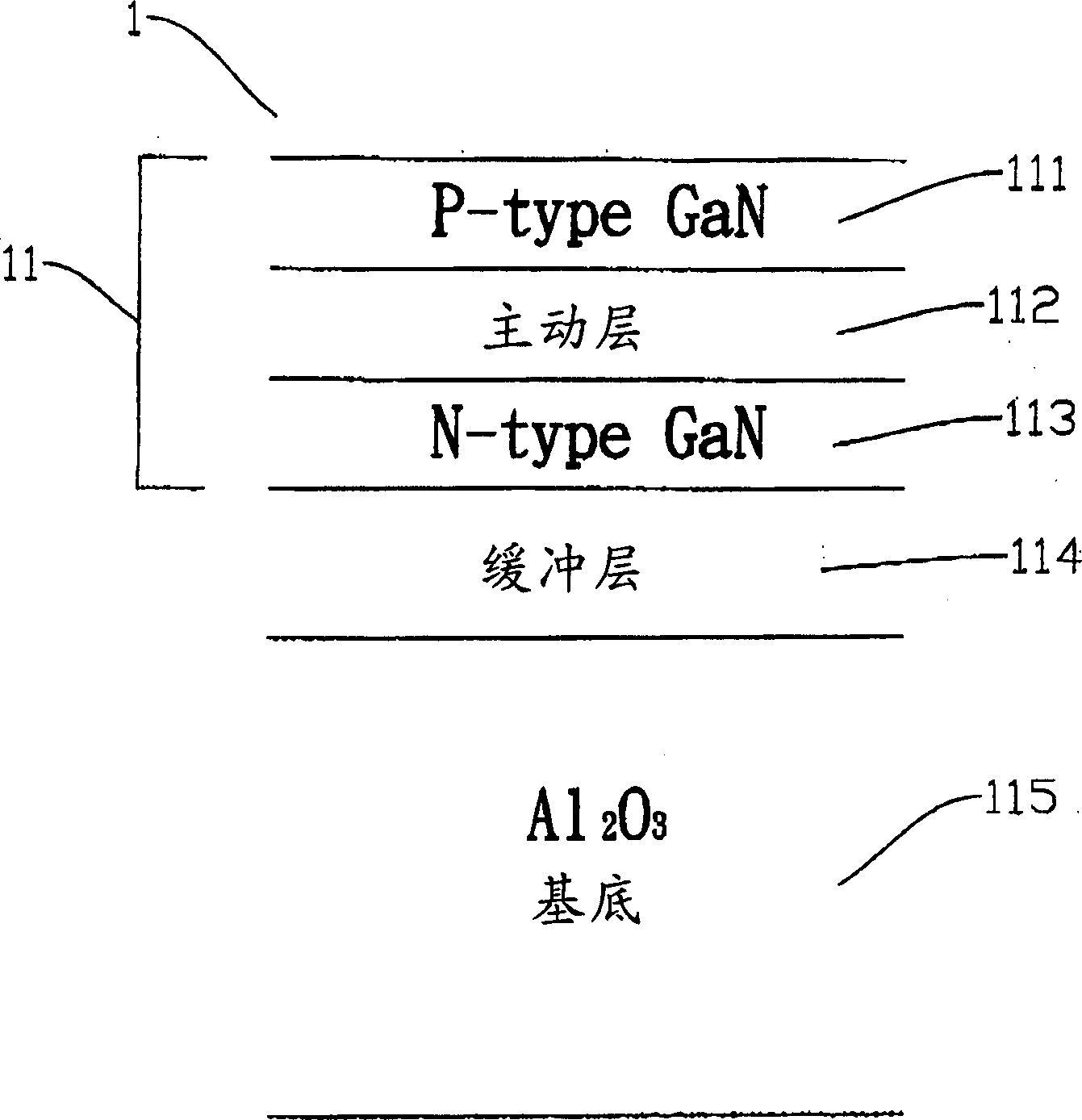
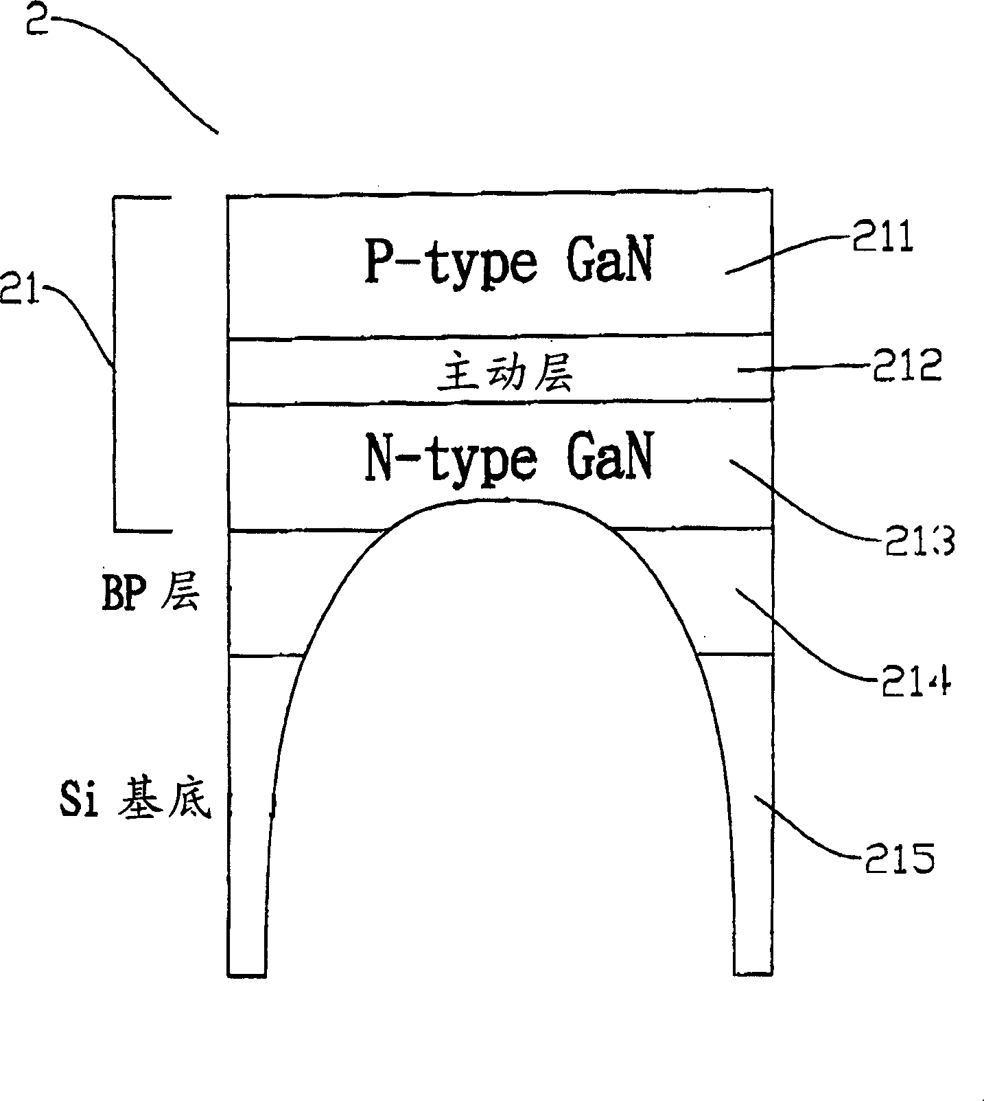
[0040] 21: components (devices)
[0041] 211: Second confinement layer (P-type GaN layer)
[0042] 212: Active layer
[0043] 213: The first confinement layer (N-type GaN layer)
[0044] 214: Boron monophosphide layer
[0045] 215: Silicon substrate (Si(100) substrate)
Embodiment 2
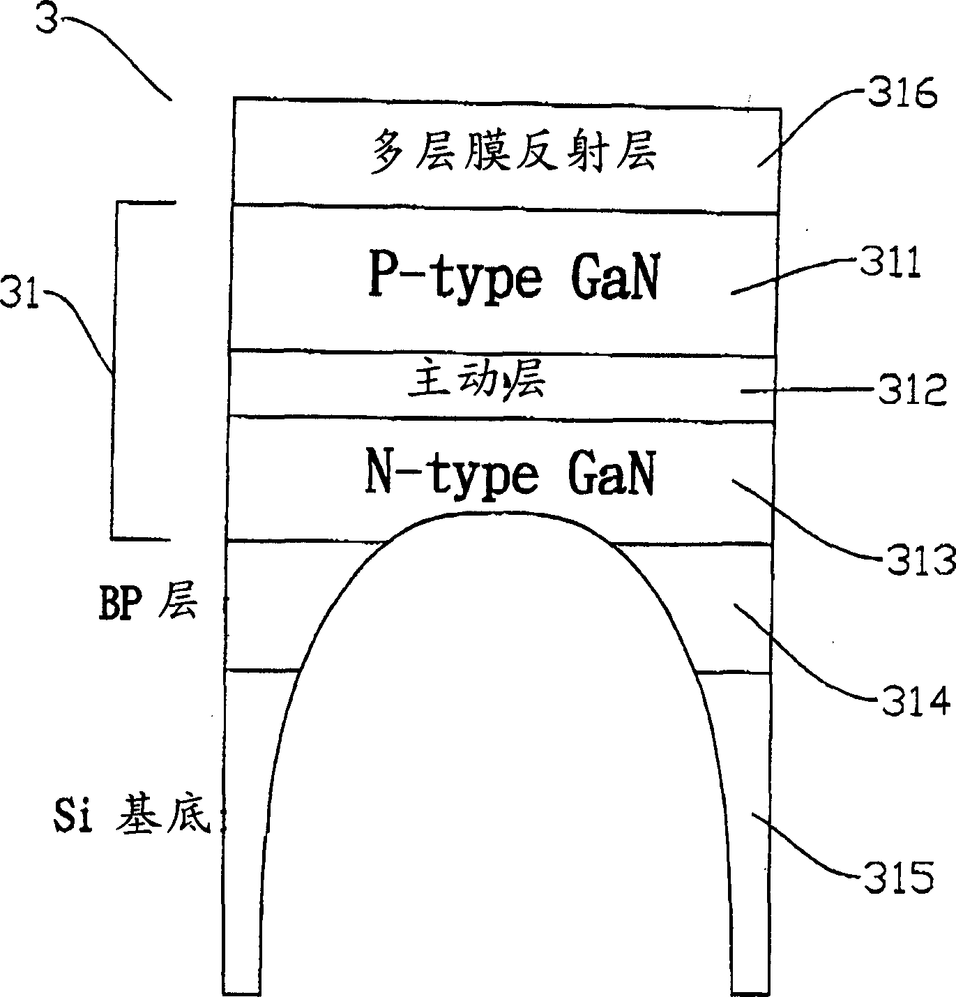
[0047] 31: components (devices)
[0048] 311: Second confinement layer (P-type GaN layer)
[0049] 312: Active layer
[0050] 313: The first confinement layer (N-type GaN layer)
[0051] 314: Boron monophosphide layer
[0052] 315: Silicon substrate (Si(100) substrate)
[0053] 316: Multilayer reflective mirror (reflecting mirror)
Embodiment 3
[0055] 41: components (devices)
[0056] 411: Second confinement layer (P-type GaN layer)
[0057] 412: Active layer
[0058] 413: The first confinement layer (N-type GaN layer)
[0059] 414: Boron monophosphide layer
[0060]415: Silicon substrate (Si(100)substrate)
[0061] 417: Micro-lens
PUM
 Abstract
Description
Claims
Application Information