Methods of roughening ceramic surface

A ceramic surface, roughening technology, used in the improvement of metal adhesion of insulating substrates, manufacturing tools, welding/welding/cutting items, etc.

Inactive Publication Date: 2004-05-12
APPLIED MATERIALS INC
View PDF0 Cites 20 Cited by
  • Summary
  • Abstract
  • Description
  • Claims
  • Application Information

AI Technical Summary

Problems solved by technology

However, as shown in FIG. 2C, when the tantalum layer 206 is formed during semiconductor processing, it pulls up the underlying aluminum sacrificial layer 204, causing the aluminum layer 204 to separate from the surface 203 of the ceramic deposition ring 202.
This usually results in spalling of the double layer of Tantalum 206 and Aluminum 204
[0008] Although the nature of this failure is not yet fully understood, initial observations indicate that it occurs near the interface 203 between the aluminum sacrificial layer 204 and the ceramic deposition ring 202 rather than deep within the aluminum layer.

Method used


Image

  • Methods of roughening ceramic surface
  • Methods of roughening ceramic surface
  • Methods of roughening ceramic surface

Examples


Embodiment Construction

[0021] DETAILED DESCRIPTION OF THE PREFERRED EMBODIMENT

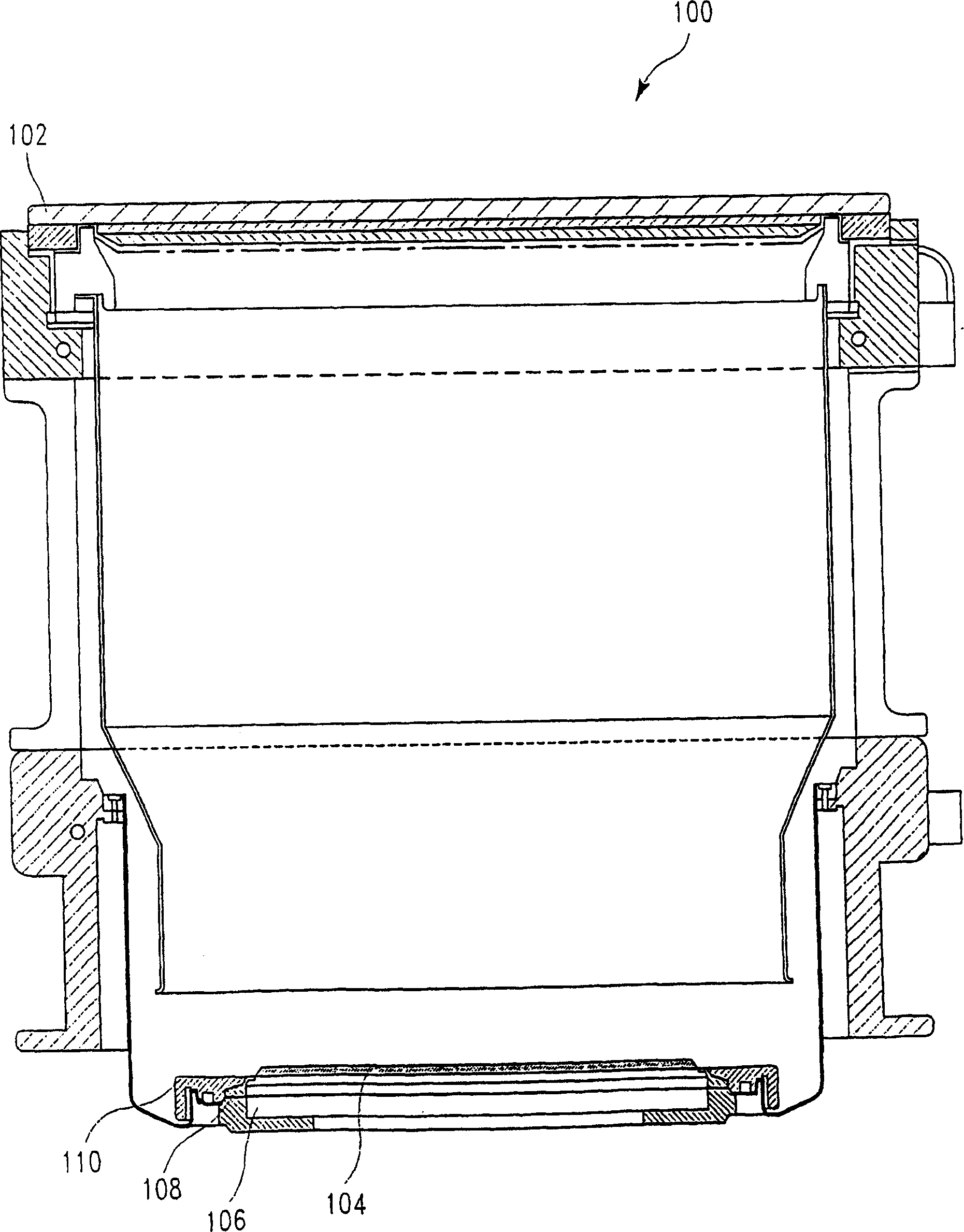
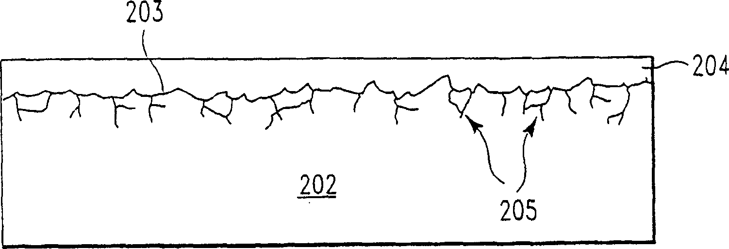
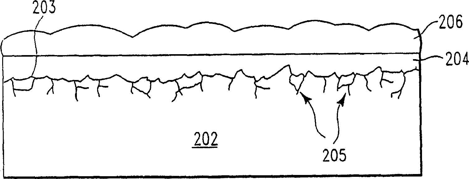
[0022] The invention discloses a method for roughening the ceramic surface by chemical etching, thermal etching, or laser micromachining to form mechanical interlocks on the ceramic surface. The method can be used to improve the adhesion of upper and lower ceramic surfaces used in semiconductor processing chambers. To illustrate the invention, applicants describe the invention as an example of use in a physical vapor deposition (PVD) chamber. Ceramic surfaces have mechanical interlocks formed by chemical etching, thermal etching, or laser micromachining. Exemplary processing conditions for carrying out the methods of the invention are listed below.

[0023] As an introduction to the Detailed Description, it should be noted that, as used in this specification and the appended claims, the singular forms "a," "an," and "the" include plural referents unless the context clearly dictates otherwise. illustra...


PUM

PropertyMeasurementUnit
diameteraaaaaaaaaa
depthaaaaaaaaaa
depthaaaaaaaaaa

Abstract

Disclosed herein is a method of roughening a ceramic surface by forming mechanical interlocks in the ceramic surface by a chemical etching process, a thermal etching process, or a laser micromachining process. Also disclosed herein are components for use in semiconductor processing chambers (in particular, a deposition ring for use in a PVD chamber) which have at least one ceramic surface having mechanical interlocks formed therein by chemical etching, thermal etching, or laser micromachining. Ceramic surfaces which have been roughened according to the chemical etching, thermal etching, or laser micromachining process of the invention are less brittle and damaged than ceramic surfaces which are roughened using conventional grit blasting techniques. The method of the invention results in a roughened ceramic surface which provides good adherence to an overlying sacrificial layer (such as aluminum).

Description

Background of the invention [0001] 1. field of invention [0002] The present invention relates to a method of roughening the surface of a ceramic to improve the adhesion of materials applied to the ceramic. The invention also relates to components comprising rough ceramic surfaces for use in semiconductor processing equipment. [0003] 2. Brief introduction of background technology [0004] In semiconductor device fabrication, physical vapor deposition (PVD) is a method often used to deposit a layer of material onto a substrate. figure 1 A schematic cross-sectional view of a PVD processing chamber 100 is shown. In the PVD process, a plasma (such as an argon plasma) is used to sputter material (such as copper or tantalum) from a target 102 onto a semiconductor substrate 104 (typically a silicon wafer) positioned above an electrostatic chuck 106 on the surface. The length of the chuck 106 extends beyond the outer edge of the semiconductor substrate 104, and a deposit...

Claims


Application Information

Patent Timeline
Patent Type & Authority Applications(China)
IPC IPC(8): B23K26/40C04B41/00C04B41/51C04B41/52C04B41/53C04B41/80C04B41/88C04B41/89C04B41/91C23C14/56H01L21/203H05K3/00H05K3/38
CPCC04B41/009C23C14/564C04B41/88C04B41/0072C04B41/91C04B41/80C04B41/5353C04B41/51C04B41/52C04B41/89C04B41/5155B23K26/408B23K26/40B23K2103/52C04B41/53C04B41/5133C04B35/10C04B35/00
Inventor E·C·韦尔登Y·何H·王C·C·斯托
Owner APPLIED MATERIALS INC
Why Eureka
Try Eureka