Electronic circuit installation wiring substrate manufacturing method based on lead-free soldering tin

A wiring substrate and lead-free solder technology are applied in the field of manufacturing wiring substrates for electronic circuit installation based on lead-free solder

Inactive Publication Date: 2004-06-16
KK TOSHIBA
View PDF0 Cites 1 Cited by
  • Summary
  • Abstract
  • Description
  • Claims
  • Application Information

AI Technical Summary

Problems solved by technology

[0011] The present invention is proposed in order to solve the above-mentioned problems in the process design and mass production of electronic circuit mounting wiring substrates using lead-free solder, and its purpose is to make electronic circuits mounted using lead-free solder that do not cause environmental problem

Method used


Image

  • Electronic circuit installation wiring substrate manufacturing method based on lead-free soldering tin
  • Electronic circuit installation wiring substrate manufacturing method based on lead-free soldering tin
  • Electronic circuit installation wiring substrate manufacturing method based on lead-free soldering tin

Examples


Embodiment 1

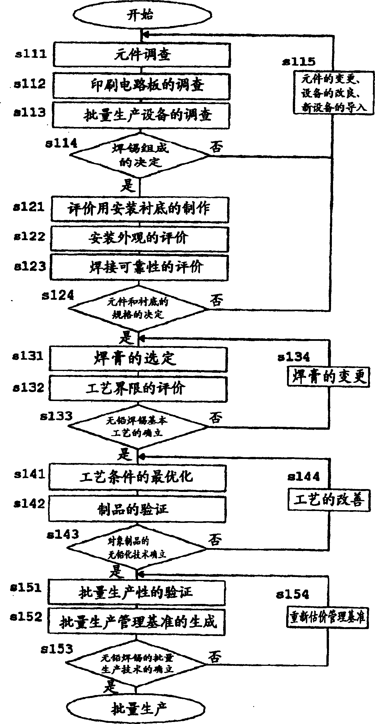
[0075] [Example 1: Reflow installation]

[0076] Below, refer to figure 1 is a flowchart illustrating a method of manufacturing a wiring substrate related to reflow mounting according to the present invention. In the following description, a method of manufacturing a wiring substrate using a soldering process based on reflow mounting will be described, but the steps in this flow chart will again study the process that has entered the mass production stage, making it easier to find out the cause of soldering failures. Although it can be used to improve manufacturing yield, this flow chart can also be applied when designing a manufacturing process of a manufacturing method of a mounted wiring substrate using reflow mounting.

[0077] (s111: Component investigation and confirmation steps)

[0078] The first step (s111) is a step of investigating and confirming components to be mounted or used on the mounting wiring board. In this step, the heat-resistant conditions of the comp...

Embodiment 2

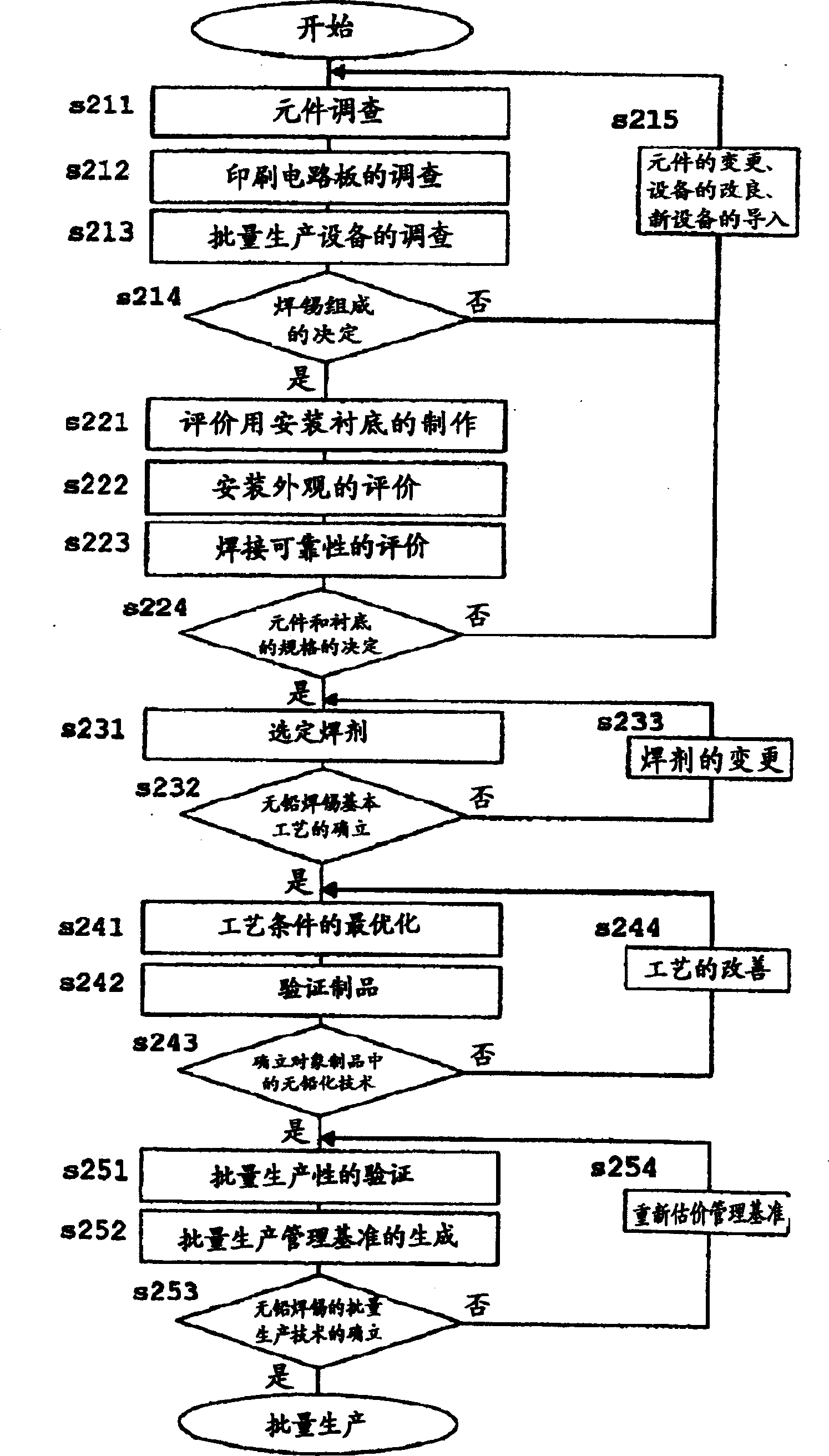
[0125] [Example 2: Process installation]

[0126] refer to figure 2The flowchart of the invention illustrates the manufacturing method of the wiring substrate related to flow mounting. In the following description, a method of manufacturing a wiring substrate using a soldering process based on flow mounting will be described, but the steps of this flow chart reconsider the process that has entered the mass production stage, so that it becomes easier to find out the cause of soldering failures. Although it can be used to improve the manufacturing yield, this flow chart can also be applied to the design of the manufacturing process of the manufacturing method of the mounted wiring substrate using flow mounting, as in the first embodiment.

[0127] (s211: Component investigation and confirmation steps)

[0128] The first step (s211) is a step of investigating and confirming components to be mounted or used on the mounting wiring board. In this step, the heat-resistant conditi...

Embodiment 3

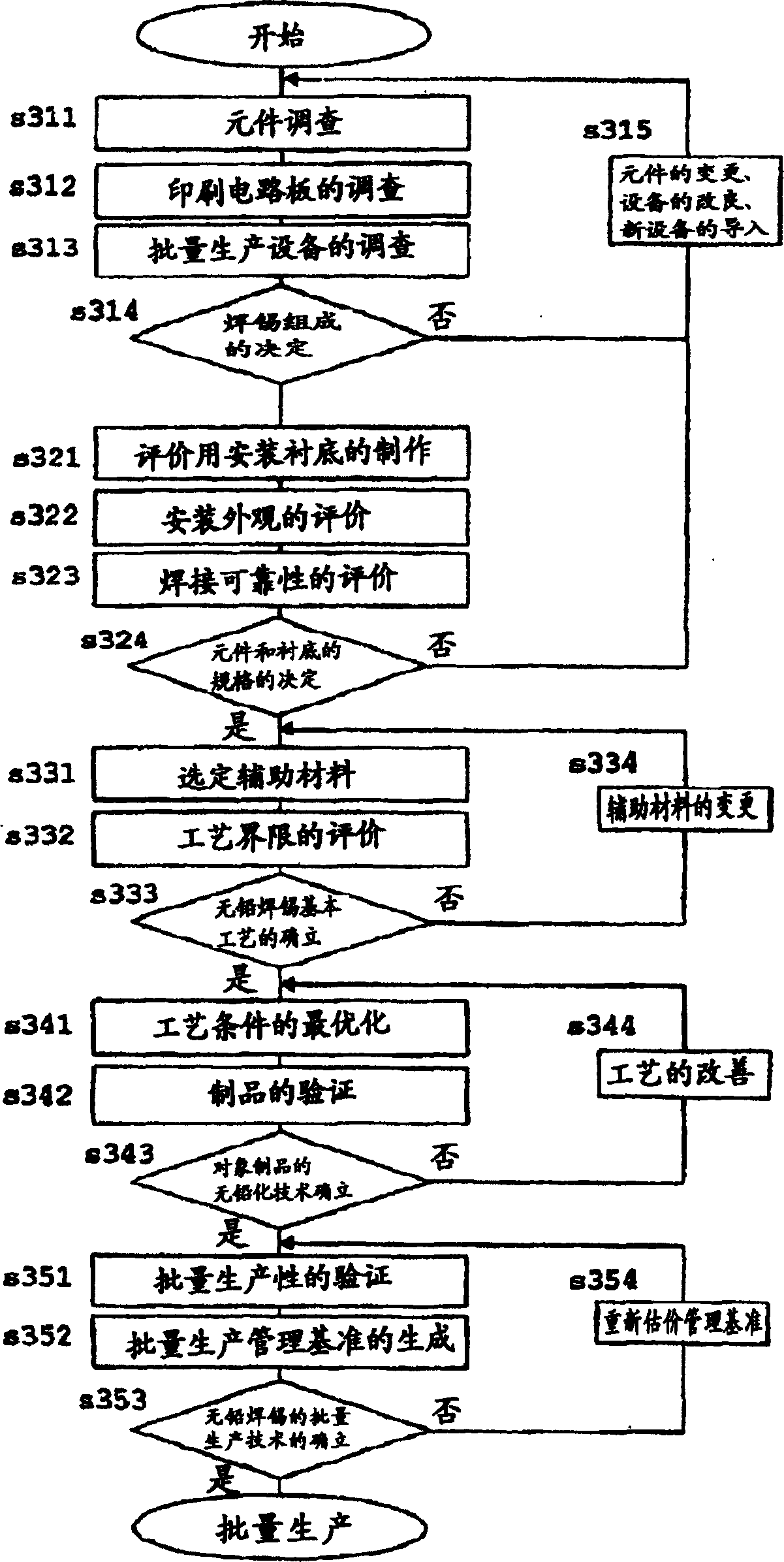
[0172] [Example 3: Hybrid installation]

[0173] refer to image 3 The flowchart of the invention illustrates the manufacturing method of the wiring substrate related to the hybrid mounting. In the following description, a method of manufacturing a wiring substrate using a soldering process based on mixed mounting will be described, but the steps of this flow chart will again study the process that has entered the mass production stage, so as to make it easier to find out the cause of soldering failures. Although it can be used to improve manufacturing yield, this flow chart can also be applied when designing a manufacturing process using a method of manufacturing a mounted wiring substrate for hybrid mounting.

[0174] (s311: Component investigation and confirmation steps)

[0175] The first step (s311) is a step of investigating and confirming components to be mounted or used on the mounting wiring board. In this step, investigate and confirm the heat-resistant conditions...


PUM


Abstract

Provided is an electronic circuit installation wiring substrate manufacturing method based on lead-free soldering tin for preventing a decrease in yield due to a defect of soldering. This manufacturing method includes a processes for investigating mounted components, investigating printed boards, investigating mass-producing facilities, determining the composition of lead-free solder according to information on them, selecting paste and flux, optimizing process conditions, judging whether or not the process conditions are practical according to the evaluation obtained through the processes; optimizing the temperature profile of soldering, verifying products, examining whether or not a solder defect is caused and judging whether or not the technique is proper as a lead-free technique, verifying mass-productivity, generating and confirming mass-production management standard, and judging whether a mass-production technique has been established in those processes.

Description

technical field [0001] The present invention relates to a method of manufacturing a mounting wiring substrate constituting an electronic circuit, and particularly relates to a method suitable for mounting using lead-free solder. Background technique [0002] Generally, in an electronic device, a wiring pattern is formed on a substrate material such as glass epoxy resin, a terminal portion for mounting an electronic component, a via hole for connecting between multilayer wiring patterns or for connecting an electronic component, etc. are used. An electronic circuit manufactured by mounting electronic components on a substrate and electrically and mechanically joining them by soldering. In addition, in this soldering step, the heating temperature needs to be higher than the melting temperature of the solder and lower than the heat-resistant temperature of the mounted electronic component. [0003] However, conventionally, Sn-Pb eutectic solder has been used as a solder materi...

Claims


Application Information

Patent Timeline
IPC IPC(8): H05K3/34
CPCH05K1/0266H05K3/3463H05K3/3485
Inventor 馆山和树森郁夫伊藤寿津田达也
Owner KK TOSHIBA
Why Eureka
Try Eureka