Method of utilizing focused ion beam in exposing required layer in failure analysis of multilayer semiconductor

A focused ion beam, semiconductor technology, applied in the field of failure analysis, can solve the problems of easy damage, low defect detection rate, troublesome and expensive

Inactive Publication Date: 2004-06-23
WINBOND ELECTRONICS CORP
View PDF1 Cites 20 Cited by
  • Summary
  • Abstract
  • Description
  • Claims
  • Application Information

AI Technical Summary

Problems solved by technology

[0003] However, if the defect is generated at the front end or the first step, such as a gate oxide layer defect, even though we can detect the failed integrated circuit through electrical analysis, it is difficult to find the source of such defects through physical property analysis. Existing methods use focused ion beam and transmission electron microscope (transmission electron microscope, TEM) to inspect gate oxide layer defects, but these tools can only detect the longitudinal section of the gate oxide layer, and the results obtained are relatively low. Defect detection rate. In addition, in deep sub-micron fabrication technology, the gate oxide layer of integrated circuits becomes thinner and more easily damaged. For example, the plasma process or electrostatic effect in the production may destroy the gate oxide layer. Floor
[0004] US Patent No. 5,935,870 titled "Preparation Method for Upward-Looking Transmission Electron Microscope Specimen" by Lee discloses a physical failure analysis method, which is to expose the gate oxide layer in the integrated circuit. Lee's method is to use chemical Mechanical polishing (CMP), etching, and ion milling to remove other layers above the gate oxide, but this method is cumbersome and expensive

Method used


Image

  • Method of utilizing focused ion beam in exposing required layer in failure analysis of multilayer semiconductor
  • Method of utilizing focused ion beam in exposing required layer in failure analysis of multilayer semiconductor
  • Method of utilizing focused ion beam in exposing required layer in failure analysis of multilayer semiconductor

Examples


Embodiment Construction

[0015] Reference numerals are added to the drawings to describe the embodiments of the present invention in detail. In all drawings, the same or similar elements will be represented by the same reference numerals as much as possible.

[0016] According to the present invention, there is provided a method for exposing a target layer of a multilayer semiconductor device, mainly by stripping at least one upper layer above the target layer by using a focused ion beam.

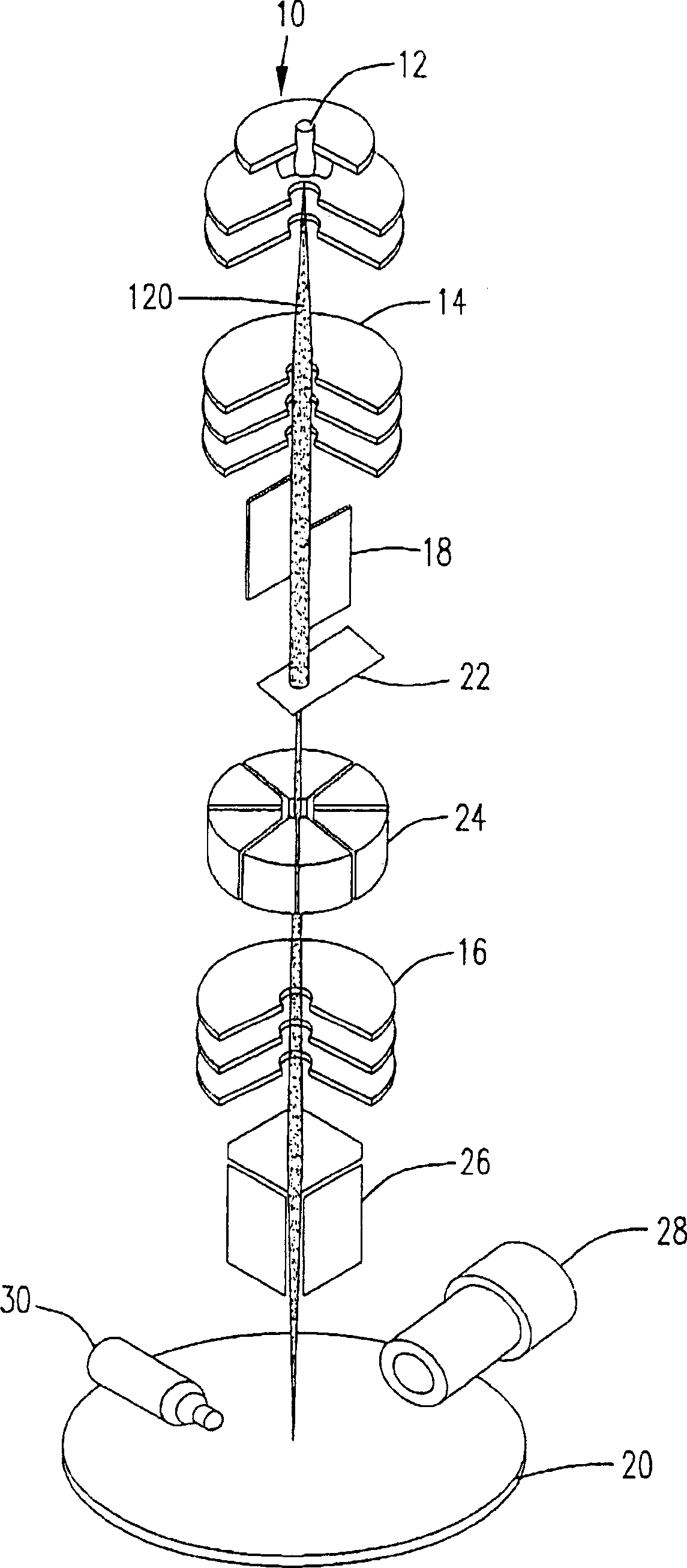
[0017] figure 1 For a description of conventional focused ion beam configurations used in the present invention, see figure 1 The focused ion beam structure 10 generally includes an ion source 12 (such as a Ga+ source), a focusing lens 14 and an objective lens 16, so that the ion beam 120 can be focused on the test piece 20 (ie, the semiconductor device herein, including a semiconductor wafer) via an ion focusing device 18 or packaged product). The focused ion beam structure 10 generally also includes an adjustab...


PUM


Abstract

The fault detecting method for semiconductor chip with several crystal grains or package includes electrical failure analysis of the semiconductor chip or package; determining the fault in at least one of several crystal grains; determining the destination layer to be analyzed in the at least one crystal grain fault; removing the layers over the determined fault crystal grain with focused ion beam apparatus; and exposing the whole destination layer for physical fault analysis.

Description

technical field [0001] The present invention relates to a failure analysis of a semiconductor device, in particular to a method for exposing desired layers in a multilayer semiconductor device. Background technique [0002] Regarding the failure analysis of semiconductor integrated circuits (integrated circuit, IC), techniques or tools such as scanning electron microscope (SEM) or focused ion beam (focusedion beams, FIB) have been developed for a long time, and can detect For defects generated in the post-production stage, these tools are used in electrical analysis and physical property analysis to find the root cause of defects. [0003] However, if the defect is generated at the front end or the first step, such as a gate oxide layer defect, even though we can detect the failed integrated circuit through electrical analysis, it is difficult to find the source of such defects through physical property analysis. Existing methods use focused ion beam and transmission electr...

Claims


Application Information

Patent Timeline
IPC IPC(8): G01R31/307
CPCG01R31/307
Inventor 洪文治李文彬
Owner WINBOND ELECTRONICS CORP
Why Eureka
Try Eureka