Liquid crystal display device with pixel of small leakage current

A liquid crystal display device, pixel technology, applied in static indicators, cathode ray tube indicators, optics, etc., can solve problems such as increased voltage stress, reliability of insulating film, difficulty in suppressing leakage current, etc. effects of stress, improved retention characteristics, and improved operational reliability

Inactive Publication Date: 2004-08-04
MITSUBISHI ELECTRIC CORP
View PDF1 Cites 12 Cited by
  • Summary
  • Abstract
  • Description
  • Claims
  • Application Information

AI Technical Summary

Problems solved by technology

[0007] However, according to the pixel structure described in JP-A-5-127619, if the display voltage becomes higher, it becomes difficult to suppress the leakage current.
And the structure of controlling the gate voltage for applying a strong reverse bias voltage on the TFT element during the non-scanning period has also been disclosed, but in this case because the voltage stress on the gate insulating film increases, the reliability of the insulating film will be reduced. become a problem

Method used


Image

  • Liquid crystal display device with pixel of small leakage current
  • Liquid crystal display device with pixel of small leakage current
  • Liquid crystal display device with pixel of small leakage current

Examples


Embodiment 1

[0023] (Overall structure of liquid crystal display device)

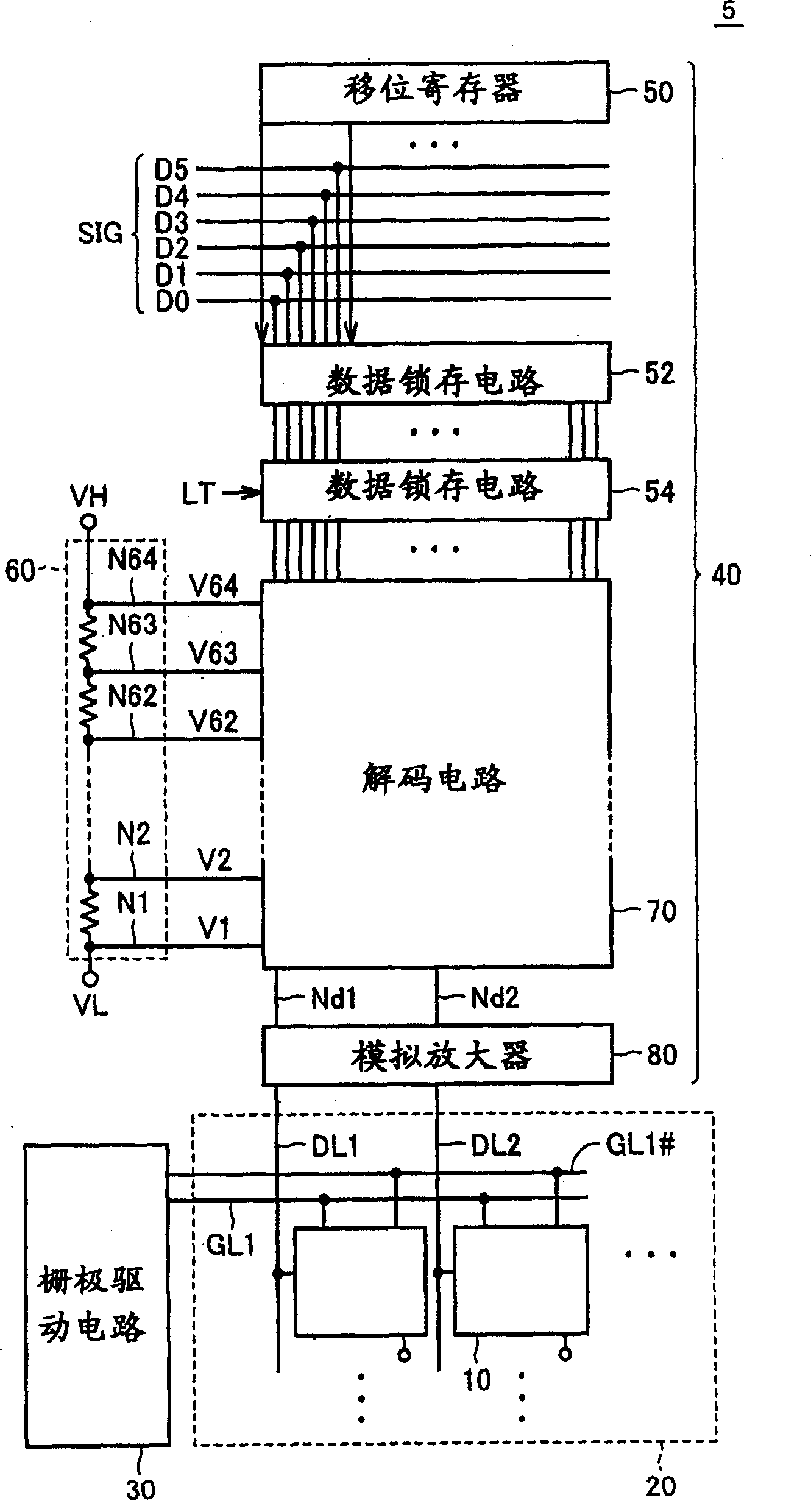
[0024] Firstly, the overall structure of the liquid crystal display device according to the embodiment of the present invention will be described.

[0025] refer to figure 1 , the liquid crystal display device 5 of the present invention includes a liquid crystal array portion 20 , a gate driving circuit 30 and a source driving circuit 40 . The liquid crystal array section 20 includes a plurality of pixels 10 arranged in rows and columns. The first gate line GL and the second gate line GL# are arranged respectively corresponding to the row of pixels (hereinafter also referred to as “pixel row”). The data lines DL are provided corresponding to columns of pixels (hereinafter also referred to as “pixel columns”). figure 1 , representatively show the pixels in the first column and the second column of the first row, and the corresponding gate lines GL1, GL1# and data lines DL1, DL2.

[0026] In order to set each gate...

Embodiment 2

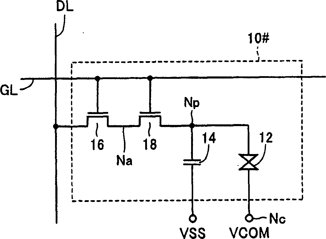
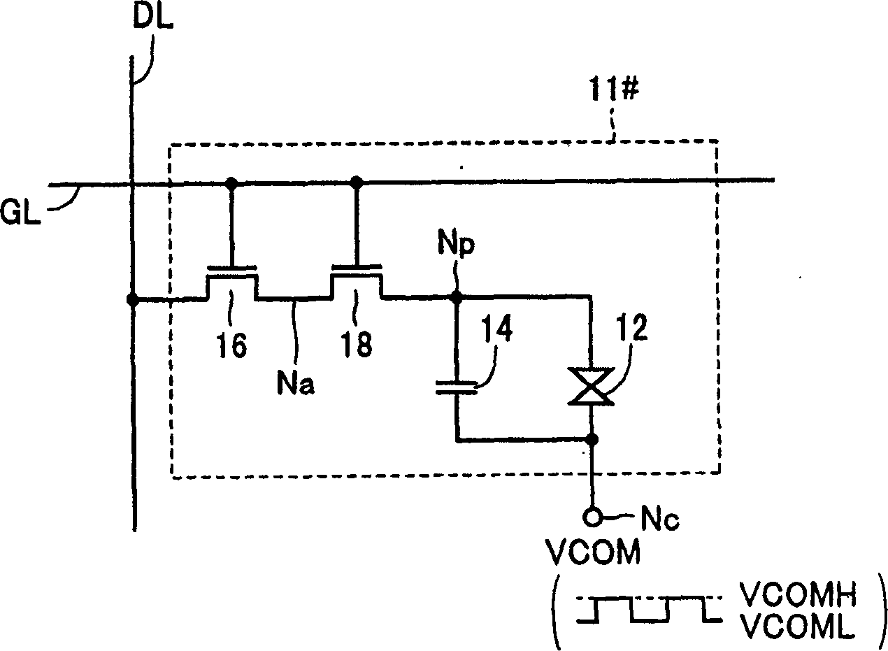
[0121] Figure 7 It is an equivalent circuit diagram showing an example of the pixel structure of the second embodiment.

[0122] exist figure 1 shown in the general diagram Figure 7 The pixel 11 shown can be used instead of the pixel 10 .

[0123] refer to Figure 7 , the pixel 11 of embodiment 2 and Figure 6 Compared with the pixel 10 of the first embodiment shown, the difference lies in that the holding capacitor 14 is connected between the pixel electrode node Np and the counter electrode node Nc. Additionally, with image 3 Similarly, the common voltage VCOM of the counter electrode node Nc is supplied as an AC voltage with an amplitude VD alternately set to the low voltage VCOML or the high voltage VCOMH at a predetermined cycle. Pixel 11 is in image 3 The pixel 11# of the shown comparative example is configured by adding an N-type TFT element 19 .

[0124] and Figure 4Like the pixel 10 shown, the gates of the N-type TFT elements 16 and 18 are connected to t...

Embodiment 3

[0146] In Embodiment 1 and Embodiment 2, it was explained that by providing a TFT element whose gate voltage is set to an intermediate voltage VGM in a non-selected state in the leakage current path, it is possible to suppress the leakage current and protect the gate insulating film of the TFT element at the same time. pixel structure.

[0147] However, although this is an ideal structure from the viewpoint of protecting the TFT element during normal operation, it cannot be used in the accelerated test (burn-in test) for intentionally applying a stress greater than normal operation to identify defects. Apply the desired stress to the component. In this burn-in test, the test is carried out under stricter conditions than the normal operation, that is, the operation test is performed by applying high temperature and large voltage stress for a predetermined time. Therefore, in order to conduct efficient tests, it is best to use a A structure that provides sufficient voltage stre...


PUM


Abstract

A pixel (10) has N type TFT elements (16, 18, 19) which are connected in series between a data line (DL) and a pixel electrode node (Np). While the gates of the TFT elements (16 and 18) are connected to a gate line (GL), the gate of the TFT element (19) is connected to a gate line (GL#). The gate lines (GL and GL#) in a selected state are set to a high voltage with which the TFT elements (16, 18, 19) can sufficiently be turned on. The gate line (GL) in an unselected state is set to a low voltage with which the TFT elements (16 and 18) can sufficiently be turned off and the gate line (GL#) in the unselected state is set to an intermediate voltage between the highest voltage and the lowest voltage which are applied through the data line (DL).

Description

technical field [0001] The present invention relates to a liquid crystal display device, in particular to a liquid crystal display device with gate insulation type field effect transistors on each pixel. Background technique [0002] The display screens of personal computers, television receivers, mobile phones, and portable information terminal devices all use liquid crystal display devices with liquid crystal elements on display pixels. This type of liquid crystal display device is more effective in reducing power consumption and size and weight than conventional liquid crystal display devices. [0003] The display brightness of the liquid crystal element changes depending on the level of the applied voltage (the voltage applied to the liquid crystal element is also referred to as "display voltage" below). The display screen of a liquid crystal display device is composed of pixels each having a liquid crystal element, and each pixel receives a display voltage in a scannin...

Claims


Application Information

Patent Timeline
Patent Type & Authority Applications(China)
IPC IPC(8): G02F1/133G09G3/20G09G3/36G09G5/10
CPCG09G2300/0814G09G2320/0214G09G2300/0809G09G3/3659G02F1/133
Inventor 飞田洋一
Owner MITSUBISHI ELECTRIC CORP
Why Eureka
Try Eureka