
Plasma processing device, annular element and plasma processing method

A ring-shaped component and plasma technology, which is applied in semiconductor/solid-state device manufacturing, electrical components, gaseous chemical plating, etc., can solve problems such as hindering the common use of processing chambers, increasing operating costs, and difficulty in shrinking, and achieving the effect of common use

Inactive Publication Date: 2004-08-18
TOKYO ELECTRON LTD
View PDF3 Cites 13 Cited by
  • Summary
  • Abstract
  • Description
  • Claims
  • Application Information

AI Technical Summary

Problems solved by technology

Even if the type of film is different, the basic components of the etching equipment are the same, so it is a good countermeasure to share the processing chamber, but for this reason, the common use of the processing chamber is hindered.
[0012] For this reason, as a reason that it is difficult to reduce the usable floor area (the area occupied by the device), and in order to increase the variation of the device, from the viewpoint of the mass production of the device and the management of the device, it becomes one of the reasons for the increase of the device manufacturing and operating costs. factor

Method used


Image

  • Plasma processing device, annular element and plasma processing method
  • Plasma processing device, annular element and plasma processing method
  • Plasma processing device, annular element and plasma processing method

Examples


Embodiment Construction

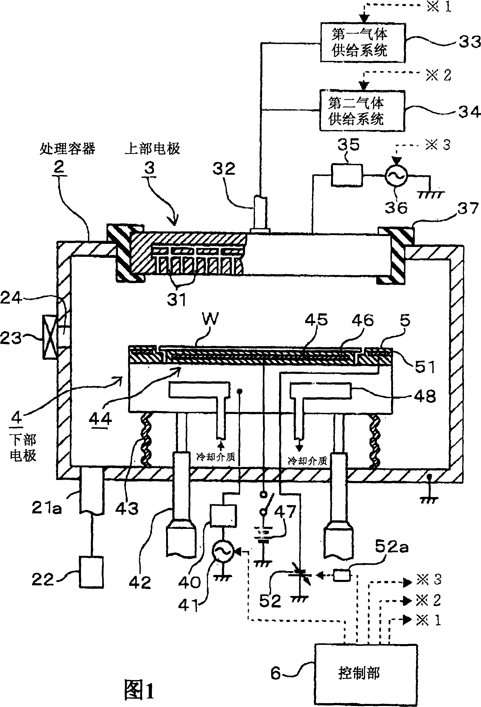
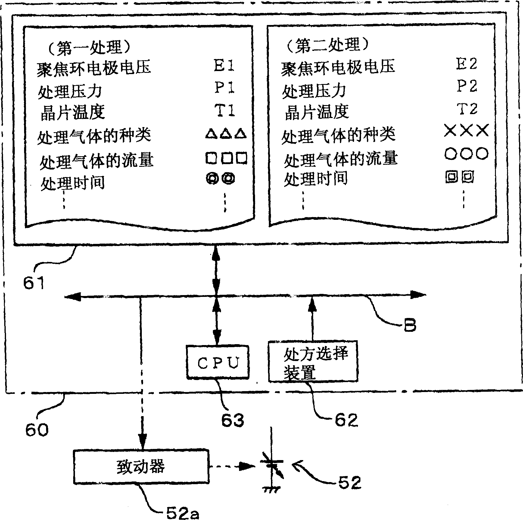
[0085] An embodiment of a plasma processing apparatus according to the present invention will be described with reference to FIG. 1 . figure 2 The processing container 2 is an airtight processing container made of a conductive member such as aluminum, and the processing container 2 is grounded. In the processing container 2, an upper electrode 3 serving as a gas shower head for introducing a specific processing gas such as an etching gas, and a lower electrode 4 serving as a substrate stage for carrying a substrate to be processed such as a wafer W are opposed to each other. set up. In addition, an exhaust port 21 is provided at the bottom of the processing container 2, and a vacuum exhaust device such as a vacuum pump 22 such as a turbomolecular pump and a dry pump is connected to the exhaust port 21 through an exhaust passage 21a. In addition, a freely openable valve 23 is provided on the side wall of the processing container 2, and an opening 24 for carrying in or carryin...


PUM

PropertyMeasurementUnit
thicknessaaaaaaaaaa
thicknessaaaaaaaaaa
thicknessaaaaaaaaaa

Abstract

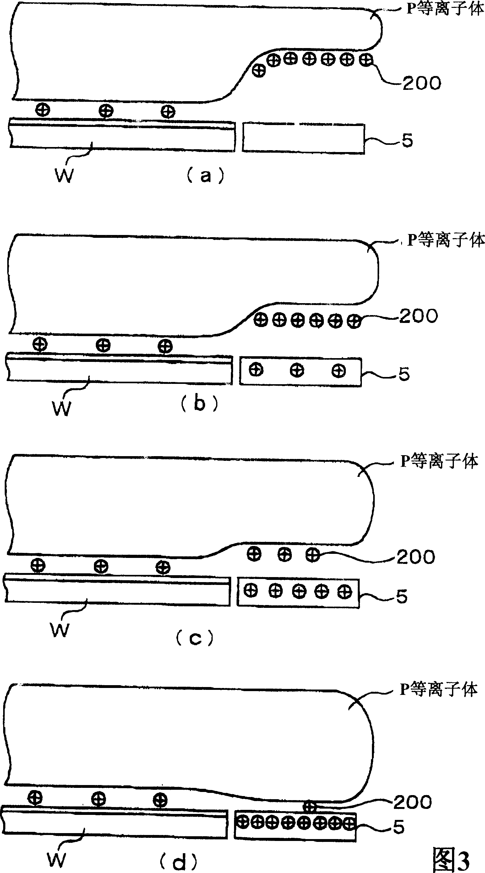
To share the use of plasma treatment apparatuses when performing a plurality of processes that are different from one another, in the plasma treatment apparatuses that use plasma, and to provide the apparatuses, ring members and a plasma treatment method that can easily align states of plasma between the apparatuses when performing the same processes by using a plurality of the apparatuses. A substrate to be treated in a treatment container is surrounded by a ring member made of an insulating material. In this ring member, electrodes are provided to adjust a plasma sheath region. When performing a first process on the substrate to be treated, for example, a first direct-current voltage is applied to the electrodes. When performing a second process on the substrate, a second direct-current voltage is applied to the electrodes. This method is applicable to a suitable direct-current voltage for each process or for each of the apparatuses performing the same processes so that the apparatuses have the same plasma conditions, enabling the shared use of the apparatuses and the easy adjustment of the plasma condition.

Description

technical field [0001] The present invention relates to a plasma processing apparatus for performing specific processing such as etching processing on a substrate such as a semiconductor wafer, for example, by plasma. Background technique [0002] Currently, in the manufacturing process of semiconductor devices, dry etching is performed on a substrate such as a semiconductor wafer (hereinafter referred to as a wafer) in order to separate capacitors and elements or to form connection holes, for example. A blade-type parallel-plate plasma processing apparatus is well known as one of apparatuses for performing such processing. (For example, refer to Patent Document 1, Patent Document 2). [0003] use Figure 28 The above-mentioned device is briefly described. This plasma device is provided with an upper electrode 11 that doubles as a gas shower head and a lower electrode 12 that doubles as a stage on the top and bottom of the airtight container 1, and surrounds the wafer W on ...

Claims


Application Information

Patent Timeline
Patent Type & Authority Applications(China)
IPC IPC(8): H01L21/3065C23C16/00C23F4/00H01J37/32H01L21/00H01L21/302
CPCH01J37/32642H01J37/32706H01L21/67069H01L21/3065
Inventor 佐佐木康晴长池宏史守屋刚
Owner TOKYO ELECTRON LTD
Learn More