High withstand voltage field effect type semiconductor device

A semiconductor and field effect technology, applied in the field of field effect semiconductor equipment, can solve problems such as poor operating performance, large switching loss, equipment damage, etc., and achieve the effects of compact switch-off characteristics, increased equipment size, and high withstand voltage performance.

Active Publication Date: 2004-09-01
TOYOTA JIDOSHA KK
View PDF0 Cites 13 Cited by
  • Summary
  • Abstract
  • Description
  • Claims
  • Application Information

AI Technical Summary

Problems solved by technology

A very long off-time itself means poor operating performance and large switching losses
Therefore, there is a high possibility of damage to the device due to heat

Method used


Image

  • High withstand voltage field effect type semiconductor device
  • High withstand voltage field effect type semiconductor device
  • High withstand voltage field effect type semiconductor device

Examples


no. 1 example

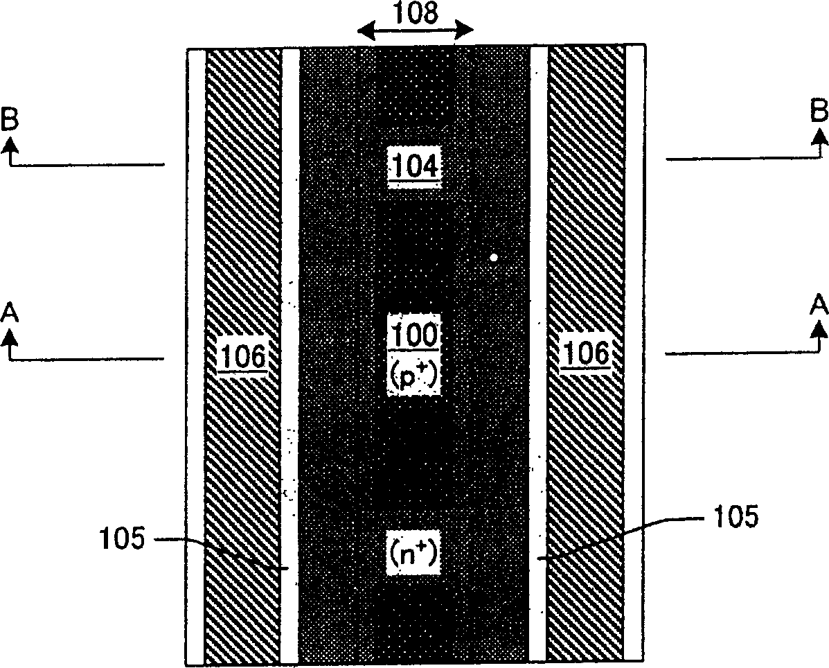
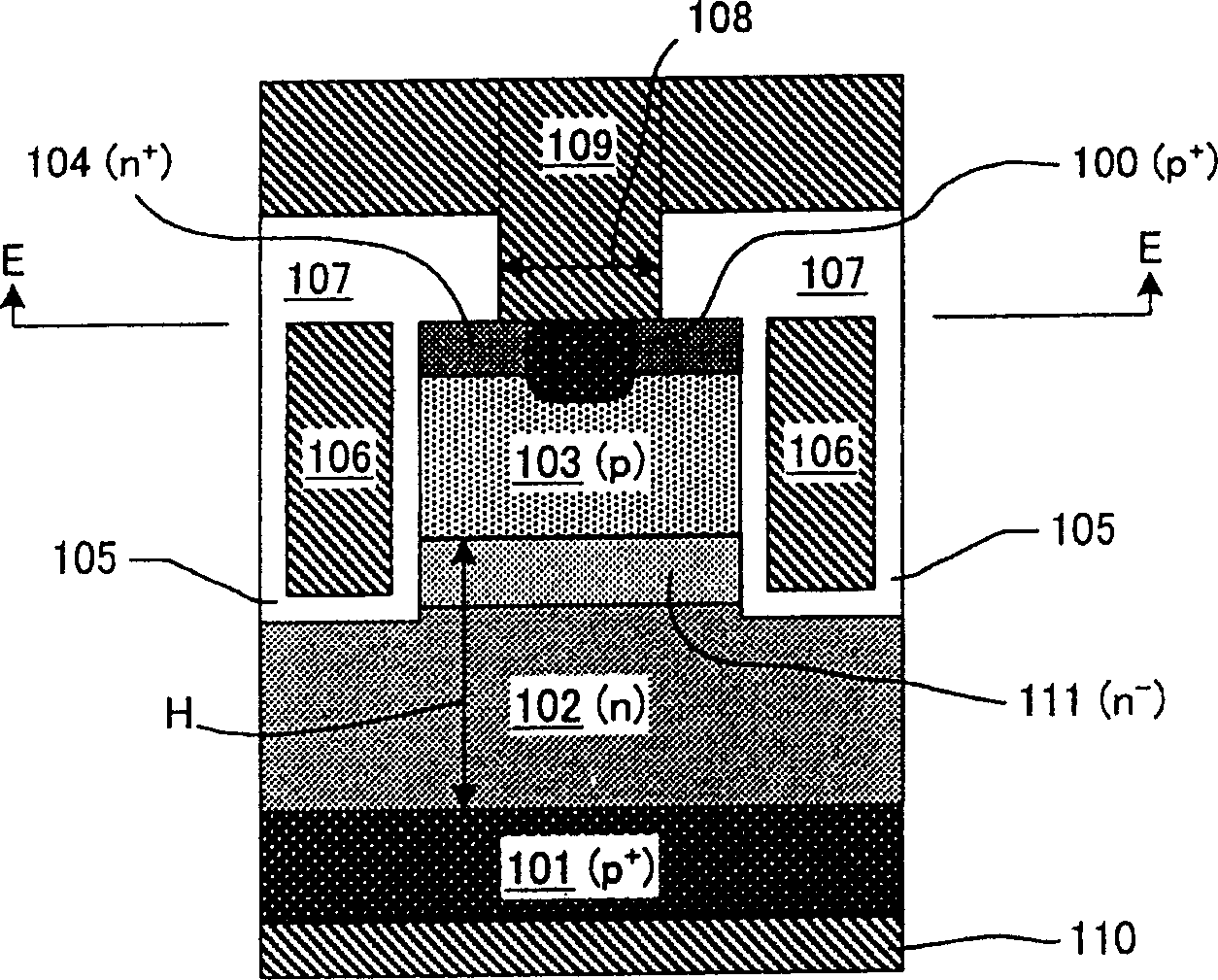
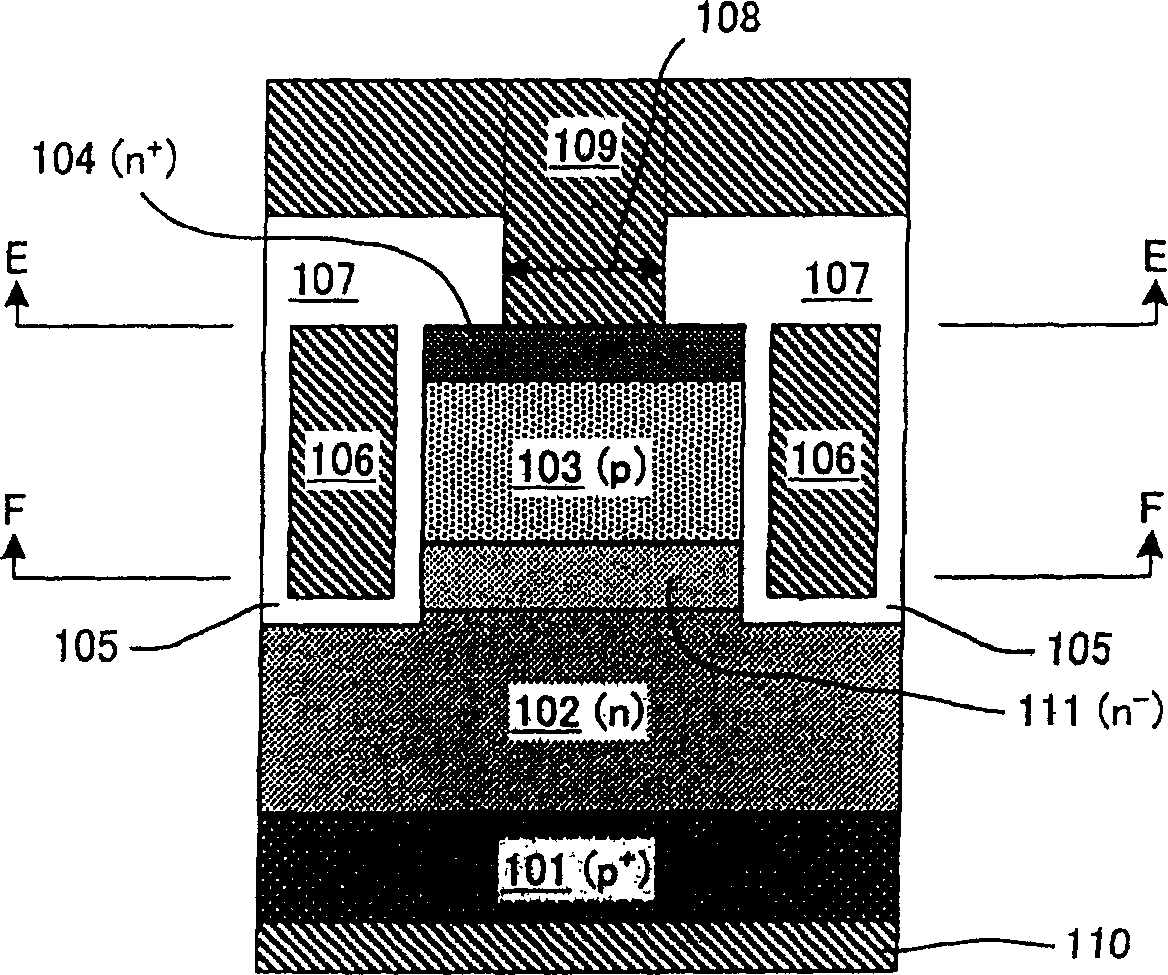
[0031] Figure 1 to Figure 3 The structure of the high withstand voltage field effect type semiconductor device according to the first embodiment is shown. figure 2 show figure 1 A cross-sectional view of part A-A. image 3 show figure 1 Sectional view of part B-B. figure 1 show figure 2 with image 3 Sectional view of part E-E in (this level is referred to as "surface" in this specification). This high withstand voltage field effect type semiconductor device is a so-called insulated gate bipolar transistor (IGBT) and has a gate electrode 106 of a channel structure. Roughly speaking, such a high withstand voltage field-effect type semiconductor device is constructed on one surface of a semiconductor substrate ( figure 2 with image 3 upper side of the middle) place N + Emitter regions 100, 104 and gate electrodes 106 and on the other surface of the substrate ( figure 2 with image 3 the lower side) to place the P + Collector region 101 etc.

[0032] That is...

no. 2 example

[0049] Figure 10 to Figure 12 A high withstand voltage field effect type semiconductor device according to the second embodiment is shown. Figure 11 show Figure 10 with Figure 12 Sectional view of part A-A in . Figure 10 show Figure 11 Sectional view of part E-E in. Figure 12 show Figure 11 Sectional view of part F-F in . in addition, Figure 10 with Figure 12 Sectional view of part B-B in and for the first embodiment of the image 3 are basically the same, except that the numbers change from "1 ** " becomes "2 ** ". In the following, it should be referenced like image 3 Interpret the numbers in this example as before. The high withstand voltage field effect type semiconductor device of this embodiment is common to that of the first embodiment in that both are of a channel type. Also, in addition to the emitter section and N - The structure of the field dispersion region and its other structures are the same as those of the first embodiment. Also, in i...

no. 3 example

[0057] Figure 13 with Figure 14 The structure of the high withstand voltage field effect type semiconductor device according to the third embodiment is shown. Figure 13 with Figure 14 Sectional view of part E-E in and for the second embodiment of Figure 10 Basically the same, except that the numbers change from "2 ** " becomes "3 ** ". In the following, it should be like when referring to Figure 10 Figures are interpreted as in this example. Figure 13 show Figure 10 A cross-sectional view of part A-A. Figure 14 show Figure 10 Sectional view of part B-B. The high withstand voltage field-effect type semiconductor device of this embodiment is common to the first and second embodiments in that they are all of the channel type. In addition, in addition to N - The structure of the field dispersion region 311 and its other structures are the same as those of the second embodiment.

[0058] N of the high withstand voltage field effect type semiconductor device of...


PUM


Abstract

It is intended to provide a high withstand voltage vertical field effect type semiconductor device that relaxes electric fields in a semiconductor substrate without thickening thickness of a drift region and achieves withstand-ability against high voltage without sacrificing ON-voltage, switch-OFF characteristics, and miniaturization. A field effect type semiconductor device comprises emitter regions (100,104) and gate electrodes (106) and the like on a surface (upper surface in FIG.2), a collector region (101) and the like on the other surface (lo - -type field dispersion regions (111) of low impurity concentration are arranged between P-type body regions (103) facing to gate electrodes (106) and an N-type drift region (102) below P-type body regions (103). Thereby, the electric field between collector and emitter is relaxed and a high withstand voltage field effect type semiconductor device is realized. Another field dispersion region can be arranged between the N-type drift region (102) and P + -type collector region (101) below the N-type drift region (102).

Description

technical field [0001] The present invention relates to a field effect type semiconductor device provided with a body region receiving a field effect of a gate electrode and a drift region disposed under the body region. More particularly, it relates to a high withstand voltage field effect type semiconductor device, which can enhance the withstand voltage performance for high voltage without sacrificing the turn-on voltage. Background technique [0002] A field effect type semiconductor device used in the prior art is used for a power supply device (for example, JP Patent Application Laid-Open No. 09-283754, etc.). Field-effect semiconductor devices of this type typically have features such as Figure 20 structure shown. Sectional drawing of parts E-E and figure 1 Basically the same, just the numbers change from "1 ** " becomes "9 ** ". In the following, it should be mentioned as figure 1 The numbers are interpreted as they are in the description of the prior art. F...

Claims


Application Information

Patent Timeline
Patent Type & Authority Applications(China)
IPC IPC(8): H01L29/78H01L21/331H01L29/06H01L29/08H01L29/739
CPCH01L29/0834H01L29/0696H01L29/7813H01L29/66348
Inventor 西胁克彦栉田知义河路佐智子
Owner TOYOTA JIDOSHA KK
Why Eureka
Try Eureka