Luminous diode array

A technology of light-emitting diodes and arrays, applied in the field of light-emitting diode arrays, can solve problems such as short circuits

Inactive Publication Date: 2004-09-08
LEXTAR ELECTRONICS CORP
View PDF2 Cites 4 Cited by
  • Summary
  • Abstract
  • Description
  • Claims
  • Application Information

AI Technical Summary

Problems solved by technology

However, in this method, only the common electrode portion is formed in the concave portion, so a short circuit caused by Au remaining on the slope of the mesa-etched trench is prone to occur.

Method used


Image

  • Luminous diode array
  • Luminous diode array
  • Luminous diode array

Examples


Embodiment Construction

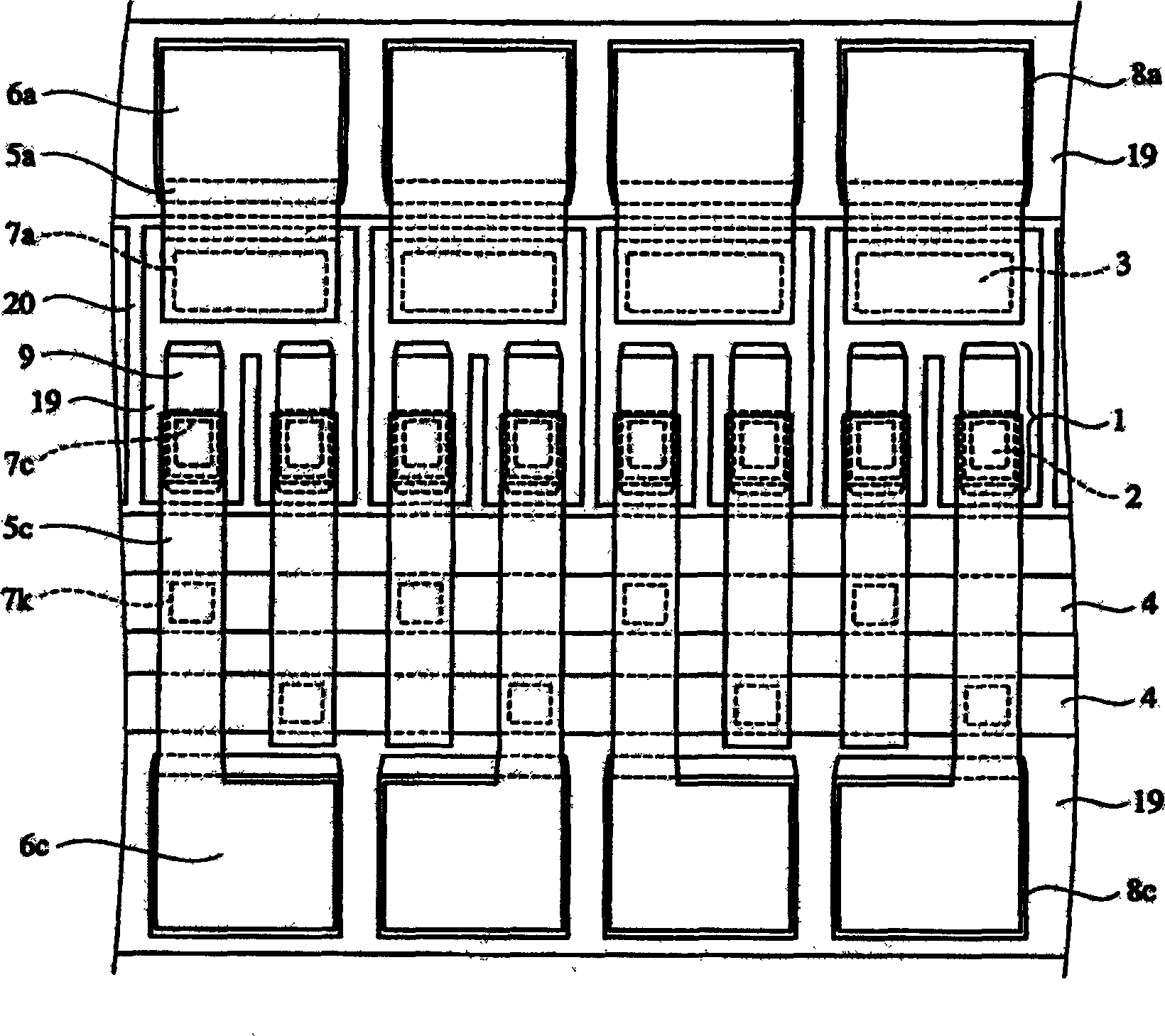
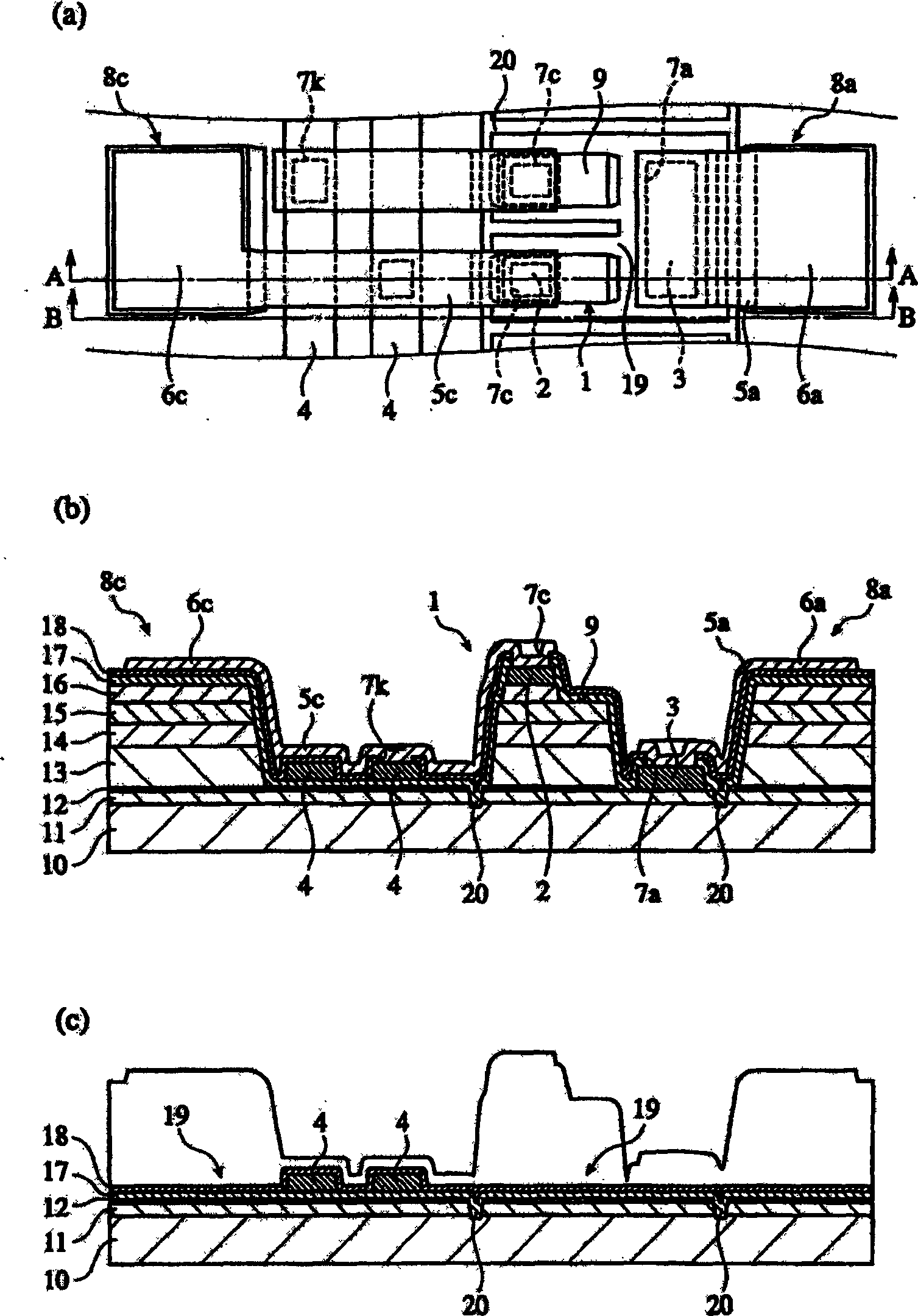
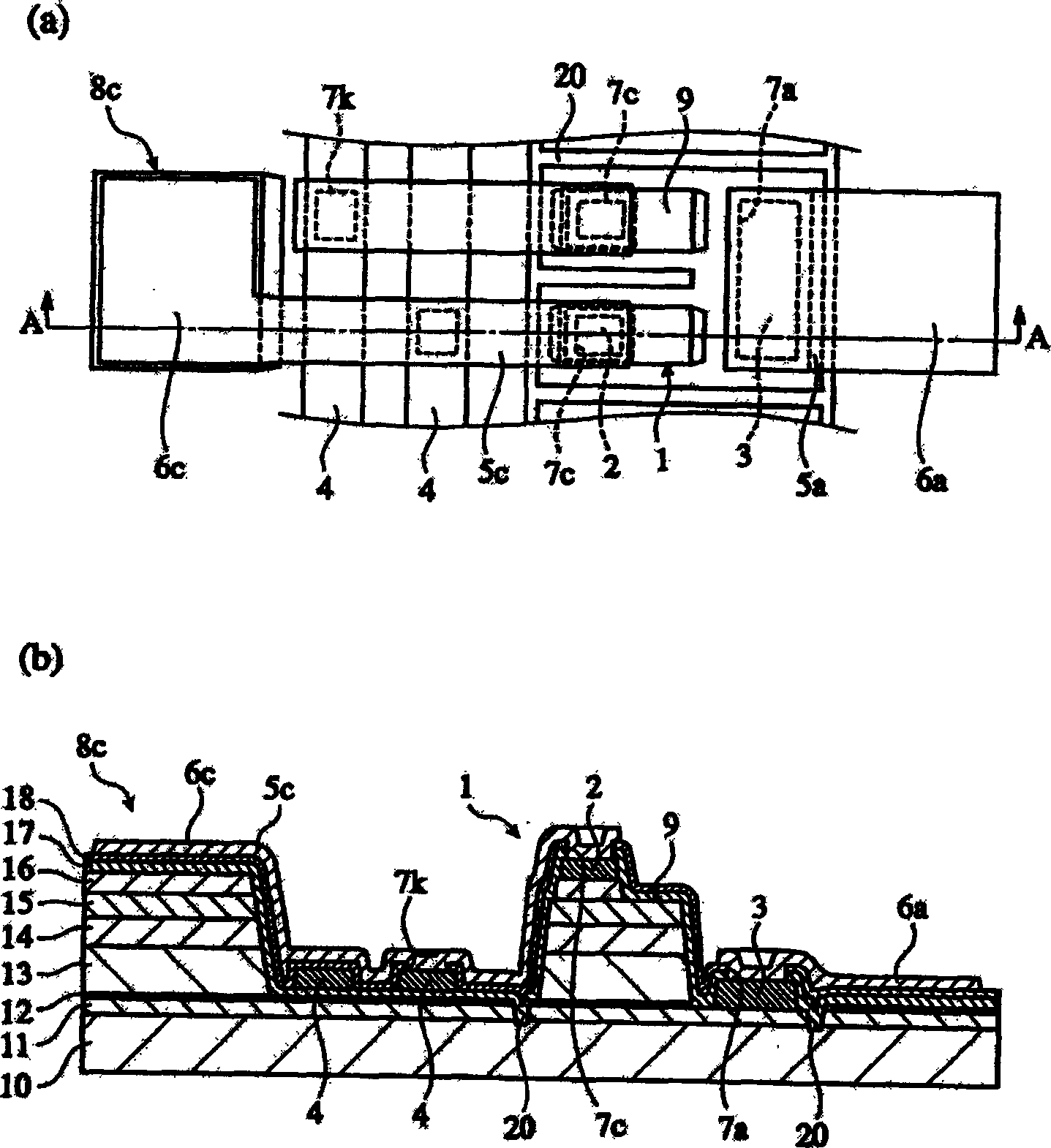
[0021] [1] Structure of LED array

[0022] Such as figure 1 and figure 2 As shown, the light-emitting diode array of the present invention has a substrate 10, a plurality of light-emitting parts 1 formed on the substrate 10, a first electrode 2 partially formed on each light-emitting part 1, and a first electrode 2 formed at a position close to the light-emitting part 1. The second electrode 3 on the conductive layer 11. In the illustrated embodiment, each light-emitting part 1 is provided with mesa etched grooves 19 and 20 on the epitaxial layer uniformly formed on the substrate 10, as each independent epitaxial layer part.

[0023] (1) Substrate

[0024] The substrate 10 is not particularly limited, as long as it can be used in a light-emitting diode and can be electrically insulated from the light-emitting part. Both the n-type substrate and the p-type substrate can be used, and semi-insulating substrates such as semi-insulating GaAs substrates or insulating substrate...


PUM


Abstract

A light-emitting diode array comprising a conductive layer formed on a substrate, separate light-emitting portions formed on the conductive layer, a first electrode formed on at least part of an upper surface of each light-emitting portion, and a second electrode formed on the conductive layer adjacent to the light-emitting portions; the first electrode comprising a common switching electrode matrix; the second electrode comprising a common electrode divided such that one second electrode exists in every block; and at least one of bonding pads extending to the first common electrode and the second common electrode being formed on a bonding portion formed on the conductive layer like an island, whereby the bonding pads are separate from each other.

Description

technical field [0001] The present invention relates to a light-emitting diode array with a large luminous output, in particular to a light-emitting diode array suitable for a light source of an electrophotography printing machine. Background technique [0002] Electrophotographic printers form an electrostatic latent image on a photosensitive drum with light corresponding to an image signal, then selectively attach resin powder to develop the image, and then transfer it to paper to obtain an image. As a light source for forming a latent image, a laser method and a light emitting diode array (arei) method are often used. In particular, the light source of the light-emitting diode array method is suitable for small printing machines and large-scale printing because it does not need to lengthen the optical path like the laser method. In recent years, with the increase in printing speed and image quality and the further miniaturization of printing machines, more high-definitio...

Claims


Application Information

Patent Timeline
Patent Type & Authority Applications(China)
IPC IPC(8): B41J2/44B41J2/45H01L27/15H01L33/08H01L33/20H01L33/30H01L33/40H01L33/44H01S5/00
CPCH01L27/153B41J2/45B65H75/28B65H75/30B65H75/4444B65H2701/34H02G11/02
Inventor 行本富久国武栄一杉山聡小森洋介助川俊光
Owner LEXTAR ELECTRONICS CORP
Why Eureka
Try Eureka