Method for lowering resistance value of cobalt disilicide layer of semiconductor devices

A technology of cobalt disilicide layer and cobalt silicide layer, which is applied in the manufacture of semiconductor/solid-state devices, circuits, electrical components, etc., and can solve the problems of component performance impact, increasing the resistance value of cobalt disilicide layer 23, leakage, etc.

Inactive Publication Date: 2004-12-08
MACRONIX INT CO LTD
View PDF0 Cites 2 Cited by
  • Summary
  • Abstract
  • Description
  • Claims
  • Application Information

AI Technical Summary

Problems solved by technology

Furthermore, if the large grains 232 of cobalt disilicide pass through the source/drain region 12 and contact the silicon substrate 10, when a voltage is applied to the semiconductor device, leakage current will also be caused.
In addition, the discontinuous region 231 produced by grain...

Method used


Image

  • Method for lowering resistance value of cobalt disilicide layer of semiconductor devices
  • Method for lowering resistance value of cobalt disilicide layer of semiconductor devices
  • Method for lowering resistance value of cobalt disilicide layer of semiconductor devices

Examples


Embodiment Construction

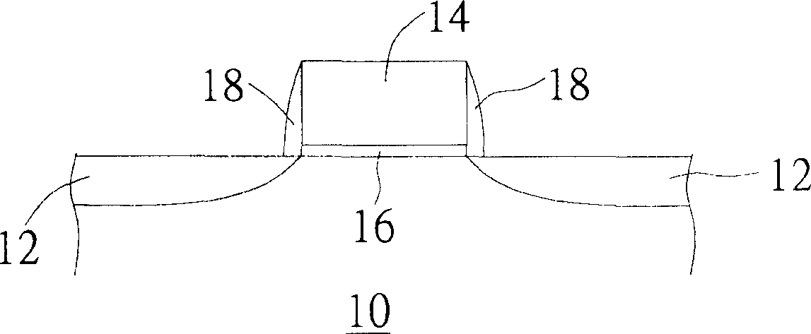
[0022] refer to Figures 2A to 2E , which shows a manufacturing method for reducing the resistance value of a cobalt disilicide layer in a semiconductor device according to a preferred embodiment of the present invention. Such as Figure 2A As shown, a silicon substrate 10 is provided first. Source / drain regions 12 are conventionally formed on the silicon substrate 10 to define a channel region. The gate 14 is mainly made of polysilicon, and is formed in the channel region and located above a gate oxide layer 16 . The sidewall buffer layer 18 is made of silicon oxide, for example, and can be formed on both sidewalls of the gate 14 .

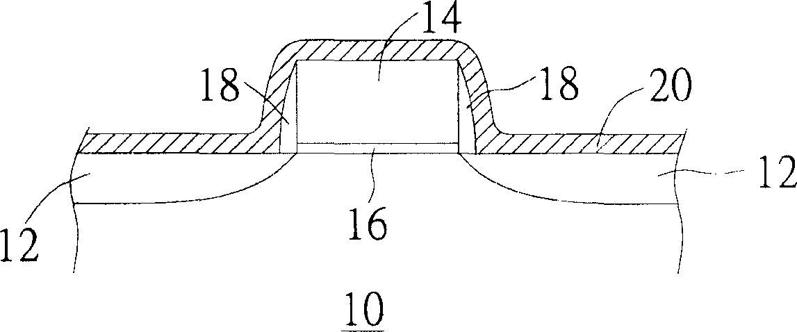
[0023] Next, if Figure 2B As shown, a metal cobalt layer 20 is formed on the silicon substrate 10 , and the metal cobalt layer 20 covers the gate 14 . The metal cobalt layer can be formed by sputtering. Thereafter, a layer of titanium or titanium nitride may be deposited on top of the metallic cobalt layer 20 (not shown) to protect the met...


PUM


Abstract

In the invention, first a layer of metal cobalt is formed on silicon substrate. Next, two times of annealing treatment are carried out. First annealing treatment turns layer of metal cobalt to layer of cobalt silicide (CoSi). Then, a covering layer in thickness of 1000-3000 Angstrom is formed to cover the layer of metal cobalt in order to restrain regrowth of crystal grain of cobalt silicide in following procedure. Finally, second annealing treatment is carried out to turn the layer of cobalt silicide to layer of disilcobalt (CoSi2).

Description

technical field [0001] The invention relates to a manufacturing method of a semiconductor component, and in particular to a method capable of reducing the resistance value of a cobalt disilicide (CoSi2) layer in the component. Background technique [0002] In the process of semiconductor components, a low-resistance cobalt disilicide (CoSi2) layer is often formed on internal electrical connection points such as gate, source or drain. Generally speaking, the manufacturing method of cobalt disilicide is to first form a metal cobalt (Co) layer on a silicon-containing substrate, and then undergo two annealing treatments (annealing treatment) to transform the cobalt into cobalt disilicide. Wherein, the first annealing treatment is to diffuse cobalt into the silicon-containing substrate to form a cobalt silicide (CoSi) layer. The second annealing treatment is to transform the cobalt silicide layer into low-resistance cobalt disilicide, so as to reduce the resistance value of the ...

Claims


Application Information

Patent Timeline
IPC IPC(8): H01L21/316H01L21/3205H01L21/324H01L21/336
Inventor 刘婉懿陈政顺
Owner MACRONIX INT CO LTD
Why Eureka
Try Eureka