Complementary metal oxide semiconductor image sensing element and producing method thereof

An oxide semiconductor, image sensing technology, used in semiconductor/solid-state device manufacturing, electrical components, image communication, etc., can solve problems such as absorption

Inactive Publication Date: 2004-12-08
AU OPTRONICS CORP
View PDF0 Cites 3 Cited by
  • Summary
  • Abstract
  • Description
  • Claims
  • Application Information

AI Technical Summary

Problems solved by technology

In addition, its design of configuring a transparent gate electrode in the photosensor can solve the problem of the sensed light being absorbed when passing thr

Method used


Image

  • Complementary metal oxide semiconductor image sensing element and producing method thereof
  • Complementary metal oxide semiconductor image sensing element and producing method thereof
  • Complementary metal oxide semiconductor image sensing element and producing method thereof

Examples


Embodiment Construction

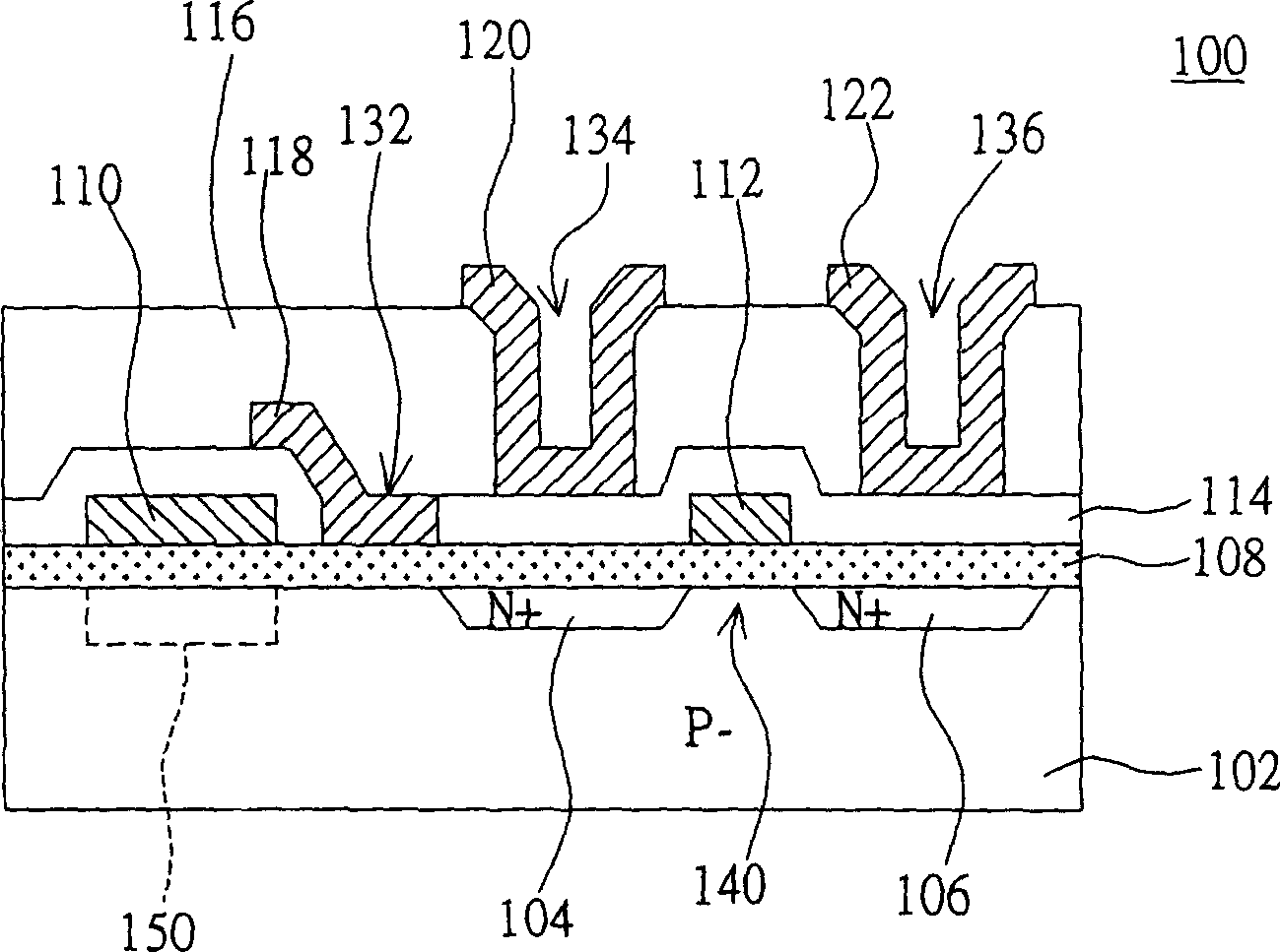
[0030]The present invention specifically designs a complementary metal oxide semiconductor (CMOS) image sensor (image sensor) and its manufacturing method, which uses a non-single-crystal-silicon-base substrate (non-single-crystal-silicon-base substrate) The design can reduce the manufacturing cost. In addition, the present invention configures a transparent gate electrode (transparent gate electrode) in the design of the photo detector (photo detector), which can solve the problem of the sensed light being absorbed when passing through the traditional polysilicon gate electrode, and reduce the sensitivity of the sensing result. error and image distortion, and improve image quality.

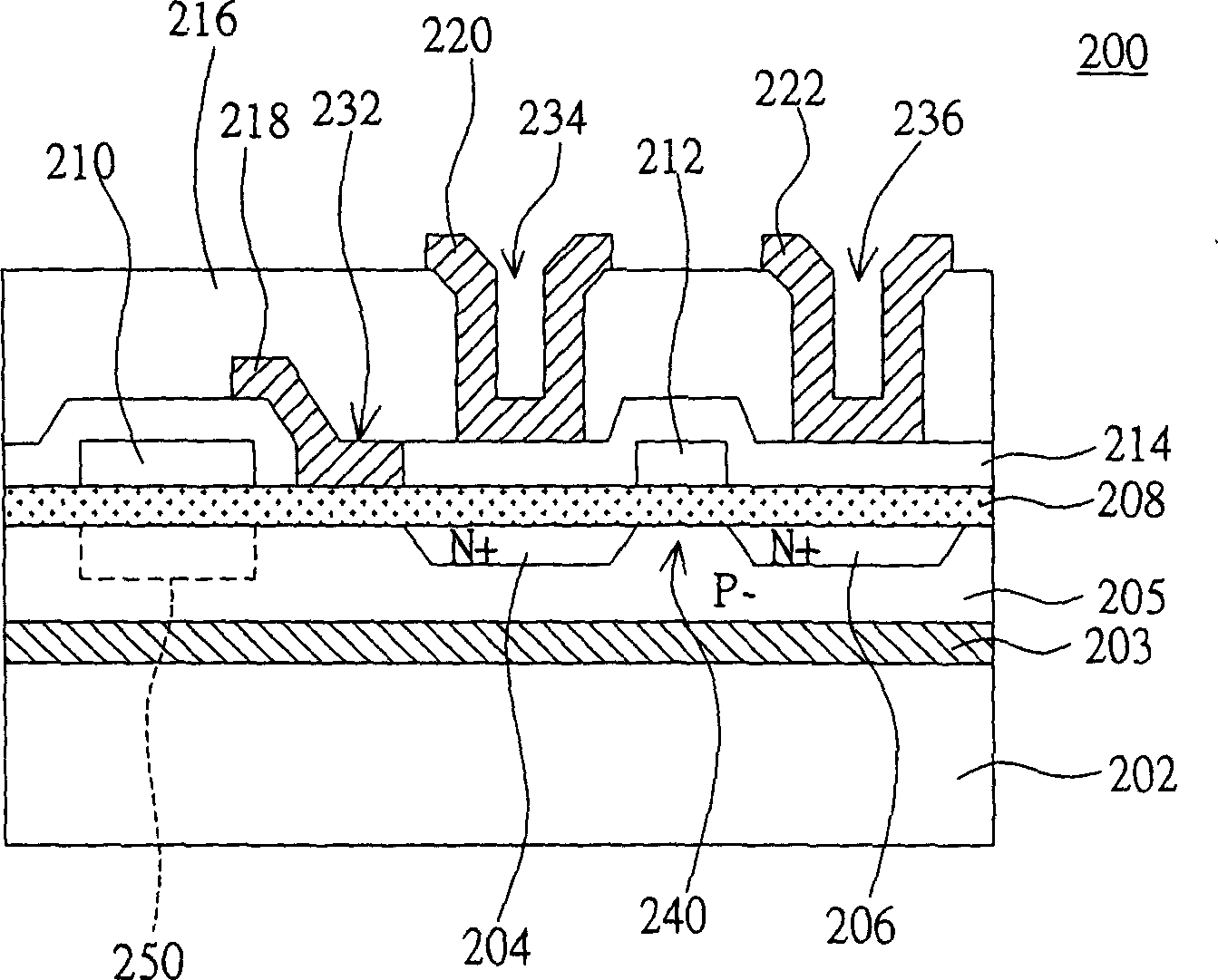
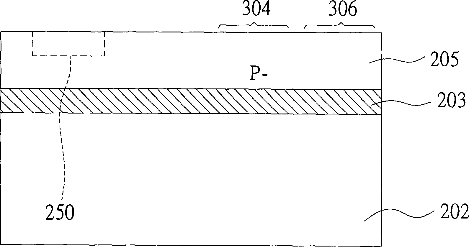
[0031] Please refer to figure 2 , which shows a cross-sectional view of a CMOS image sensing device according to a preferred embodiment of the present invention. exist figure 2 Among them, the complementary metal oxide semiconductor image sensing element 200 at least includes a non-single cr...


PUM


Abstract

The sensing component includes at least substrate of non-monocrystalline silicon, lighttight layer, polycrystalline silicon layer, source pole, drain pole, grid dielectric layer, first transparent electrode and second transparent electrode. The lighttight layer is formed on substrate of non-monocrystalline silicon, and polycrystalline silicon layer formed on the lighttight layer possesses a charge generation region. Source pole and drain pole are formed on the polycrystalline silicon layer. A prearranged channel region is formed on the polycrystalline silicon layer between source pole and drain pole, and the source pole is located between the channel region and the charge generation region. Grid dielectric layer is formed on polycrystalline silicon layer, and the first transparent electrode and the second transparent electrode formed on the grid dielectric layer are positioned above the charge generation region and the channel region respectively.

Description

technical field [0001] The present invention relates to a complementary metal oxide semiconductor (complementary metal oxide semiconductor, CMOS) image sensor (image sensor) and its manufacturing method, and in particular to a non-single-crystal-silicon substrate (non-single-crystal-silicon) -base substrate) and a complementary metal oxide semiconductor image sensing element of a transparent gate electrode and a manufacturing method thereof. Background technique [0002] In today's era of rapid technological development, image sensing devices have been widely used in televisions, toys, security systems, scanners, mobile phones, digital video cameras, digital cameras and other portable electronic products. Current image sensing devices include at least a charge coupled device (CCD) and a complementary metal oxide semiconductor image sensing device, wherein the complementary metal oxide semiconductor image sensing device has the characteristics of low cost and low power consum...

Claims


Application Information

Patent Timeline
IPC IPC(8): H01L21/822H01L27/146H04N5/335
Inventor 杨健生
Owner AU OPTRONICS CORP
Why Eureka
Try Eureka