
Quick algorithm in planar charge coupling device array super resolution imaging technology

A charge-coupled device and super-resolution technology, which is applied in electrical components, semiconductor/solid-state device manufacturing, circuits, etc., can solve problems such as processing difficulties, increasing the difficulty of imaging lens design, and expanding the field of view

Inactive Publication Date: 2004-12-15
NAT UNIV OF DEFENSE TECH
View PDF0 Cites 7 Cited by
  • Summary
  • Abstract
  • Description
  • Claims
  • Application Information

AI Technical Summary

Problems solved by technology

It can effectively increase the resolution of the system, but the splicing process requires high requirements, the system structure is very complicated, and the design difficulty of the imaging lens is increased, the field of view is expanded, and it becomes an optical system with a large field of view, and the image quality of the lens is difficult to guarantee
[0006] 3. Redesign the shape and arrangement of the charge-coupled device pixels, adopt honeycomb arrangement and polygonal shape, so that more photosensitive units with the same photosensitive area as the traditional charge-coupled device can be placed on the unit area. There are still difficulties, and the resolution improvement is limited
The above algorithms have their own advantages and disadvantages, but a common problem is that the calculation amount of the algorithm is very large, and the calculation process requires a large storage space, which is very difficult for ordinary PCs or DSP processing systems, so it is necessary to There is still a certain distance to be applied to engineering practice

Method used

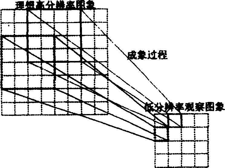
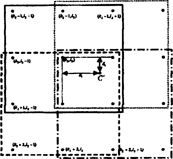
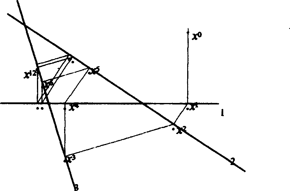

Image

  • Quick algorithm in planar charge coupling device array super resolution imaging technology
  • Quick algorithm in planar charge coupling device array super resolution imaging technology
  • Quick algorithm in planar charge coupling device array super resolution imaging technology

Examples


Embodiment Construction

[0053] The present invention is improved on the basis of studying the prior art. It proposes a pixel-level neighborhood bilinear interpolation image degradation model, proposes a four-dimensional coefficient matrix storage structure, and establishes a coefficient table by quantifying the sub-pixel displacement. , reducing the occupied space of the original model coefficients from G level to K level. At the same time, an improved Cimmino row processing iterative algorithm is proposed, and a fast algorithm for realizing super-resolution image reconstruction in the spatial domain is given. . Parallel algorithms are also given for parallel systems composed of multiple CPUs.

[0054] The algorithm steps are described below.

[0055] 1. Establish a pixel-level bilinear interpolation image degradation model:

[0056] For the convenience of comparison and description, the general airspace image degradation mathematical model is given first:

[0057] Suppose the resolution of p-fra...


PUM


Abstract

A quick algorithm relates to the technology of an area array charge coupling device hyper-resolution image by carrying out process to a multiframe picture having mutual shift to a same target to get a frame of picture with even higher resolution characterizing in setting up a pixel level adjacent domain dual linear interpolation image degraded model and applying four-dimensional non-sparse matrix to store the model factor so as to avoid memory and process to large scale sparse matrix, carrying out guantization process to the sub-pixel shift to reduce the requirement of computing process to storage space, the improved Cimmino iterative algorithm speeds up the convergence and reduces computation volume suitable for realizing PC or DSP insertion systems.

Description

Technical field: [0001] The present invention relates to the field of image imaging technology, in particular to an algorithm for the super-resolution imaging technology of an area array charge-coupled device for obtaining a frame of higher-resolution images by processing multiple frames of images with mutual displacements of the same target . Background technique: [0002] The research on super-resolution imaging technology of area array charge-coupled device (CCD for short) is of great significance. Due to the limitation of technology, the resolution of the current imaging system using charge-coupled device as the receiver always has a certain gap with many actual needs. The super-resolution imaging system can use the existing charge-coupled device to obtain images higher than its own resolution, and can achieve the purpose of obtaining high-resolution images. Especially for infrared imaging systems, due to the sensitivity problem, the pixels of infrared charge-coupled de...

Claims


Application Information

Patent Timeline
IPC IPC(8): H01L21/82H01L27/148
Inventor 吕海宝罗武胜曹聚亮周卫红楚兴春李冠章谭晓波谌廷政徐涛
Owner NAT UNIV OF DEFENSE TECH
Learn More