Method of manufacturing a photovoltaic silicon

A manufacturing method, optoelectronic technology, applied in chemical instruments and methods, semiconductor/solid-state device manufacturing, circuits, etc., can solve problems such as low production efficiency, and achieve the effect of reducing manufacturing costs

Inactive Publication Date: 2005-01-26
福建兴朝阳硅材料股份有限公司
View PDF2 Cites 15 Cited by
  • Summary
  • Abstract
  • Description
  • Claims
  • Application Information

AI Technical Summary

Problems solved by technology

Its obvious disadvantage is that the production efficiency is low

Method used


Image

  • Method of manufacturing a photovoltaic silicon

Examples


Embodiment 1

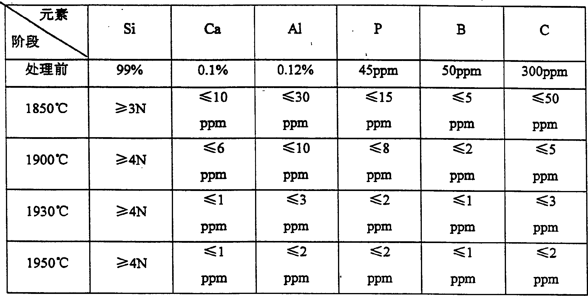
[0015] In the vacuum negative pressure chamber, use an intermediate frequency induction furnace to raise the temperature to 1850°C, melt the raw material chemical grade silicon, remove aluminum, boron, phosphorus, sulfur, carbon, etc.; under the protection of nitrogen, pass 1:1.4 into the silicon melt Water vapor and hydrogen, the amount of gas introduced can be 16Kg / min, stirred and refined for 4 hours, other elements are vaporized at high temperature and then poured into the coagulator; directional solidification is carried out from bottom to top in the vacuum negative pressure chamber to remove iron and other Heavy metals; slowly cool down to room temperature to obtain photoelectric grade silicon. A water jacket is used at the bottom of the coagulator to control the flow rate of water to achieve the purpose of slow cooling, so as to control its coagulation speed.

Embodiment 2

[0017] In the vacuum negative pressure chamber, use an intermediate frequency induction furnace to raise the temperature to 1900°C, melt the chemical grade silicon as the raw material, and remove aluminum, boron, phosphorus, sulfur, carbon, etc.; under the protection of argon, pass 1:1.5 Stir and refine for 3 hours to vaporize other elements at high temperature and pour them into the coagulator; carry out directional solidification from bottom to top in the vacuum negative pressure chamber to remove iron and other heavy metals; slowly cool down to room temperature to obtain photoelectricity grade silicon.

Embodiment 3

[0019] In the vacuum negative pressure chamber, use an intermediate frequency induction furnace to raise the temperature to 1930°C, melt the chemical grade silicon as raw material, and remove aluminum, boron, phosphorus, sulfur, carbon, etc.; Water vapor and hydrogen are stirred and refined for 3.5 hours, and other elements are vaporized at high temperature and then poured into a coagulator; directional solidification is carried out from bottom to top in a vacuum negative pressure chamber to remove iron and other heavy metals; the temperature is slowly cooled to room temperature to obtain a photoelectric grade silicon.


PUM


Abstract

Disclosed is a process for purifying photoelectric level silicon through directional freezing which consists of, melting the raw material chemical level silicon in vacuum negative pressure chamber through warming-up by an intermediate frequency induction furnace, removing aluminium, B, P, S, C and other impurity, letting water vapor and hydrogen gas into the silicon solution at the protection of inert gas, agitating homogeneously and refining, making other elements high temperature evaporate and pouring into coagulator for down-to-up directional freeze in the vacuum negative pressure chamber, eliminating ferrum and other heavy metal, and slowly cooling down to normal temperature.

Description

(1) Technical field [0001] The invention relates to the purification of silicon, in particular to a purification process of photoelectric grade silicon using directional solidification. (2) Background technology [0002] The preparation of solar cells requires high-purity silicon, which is generally required to reach 5N-7N (that is, the degree of 5-7 nines). In 1987, J.Die.l (Silicon Processing for Photovoltaics II, Elsevier Sci., Pull.B.V., 1987.285) reviewed the research results on silicon refining. In addition, in 1988, he was also at the 8th European Community Photovoltaic Solar Energy Conference Proc.sth EC Photovoltaic Solar Energy Conf., Florence, 1988.599) proposed a solar cell-grade silicon preparation process; the steps are 1) metal silicon and calcium silicate melt solution reduced by carbon in an electric furnace Mixing, so that the boron in the silicon migrates to the calcium silicate melt, and performs deboronization treatment; 2) After the treatment, the mixe...

Claims


Application Information

Patent Timeline
IPC IPC(8): C01B33/037H01L51/52
CPCH01L2251/5315H01L51/5237H10K50/84H10K2102/3026
Inventor 龚炳生
Owner 福建兴朝阳硅材料股份有限公司
Why Eureka
Try Eureka