Semi-conductor circuit arrangement

A circuit device and semiconductor technology, which is applied in the direction of electrical components, electrical signal transmission systems, instruments, etc., can solve the problem of increasing the power consumption of the modulator circuit, and achieve the effect of reducing power consumption and space requirements

Active Publication Date: 2005-03-16
INTEL CORP
View PDF0 Cites 10 Cited by
  • Summary
  • Abstract
  • Description
  • Claims
  • Application Information

AI Technical Summary

Problems solved by technology

When a semiconductor circuit device is used in a high-speed broadband signal transmission system, it must meet its high bandwidth requirements and increase the power consumption of the modulator circuit

Method used


Image

  • Semi-conductor circuit arrangement
  • Semi-conductor circuit arrangement
  • Semi-conductor circuit arrangement

Examples


Embodiment Construction

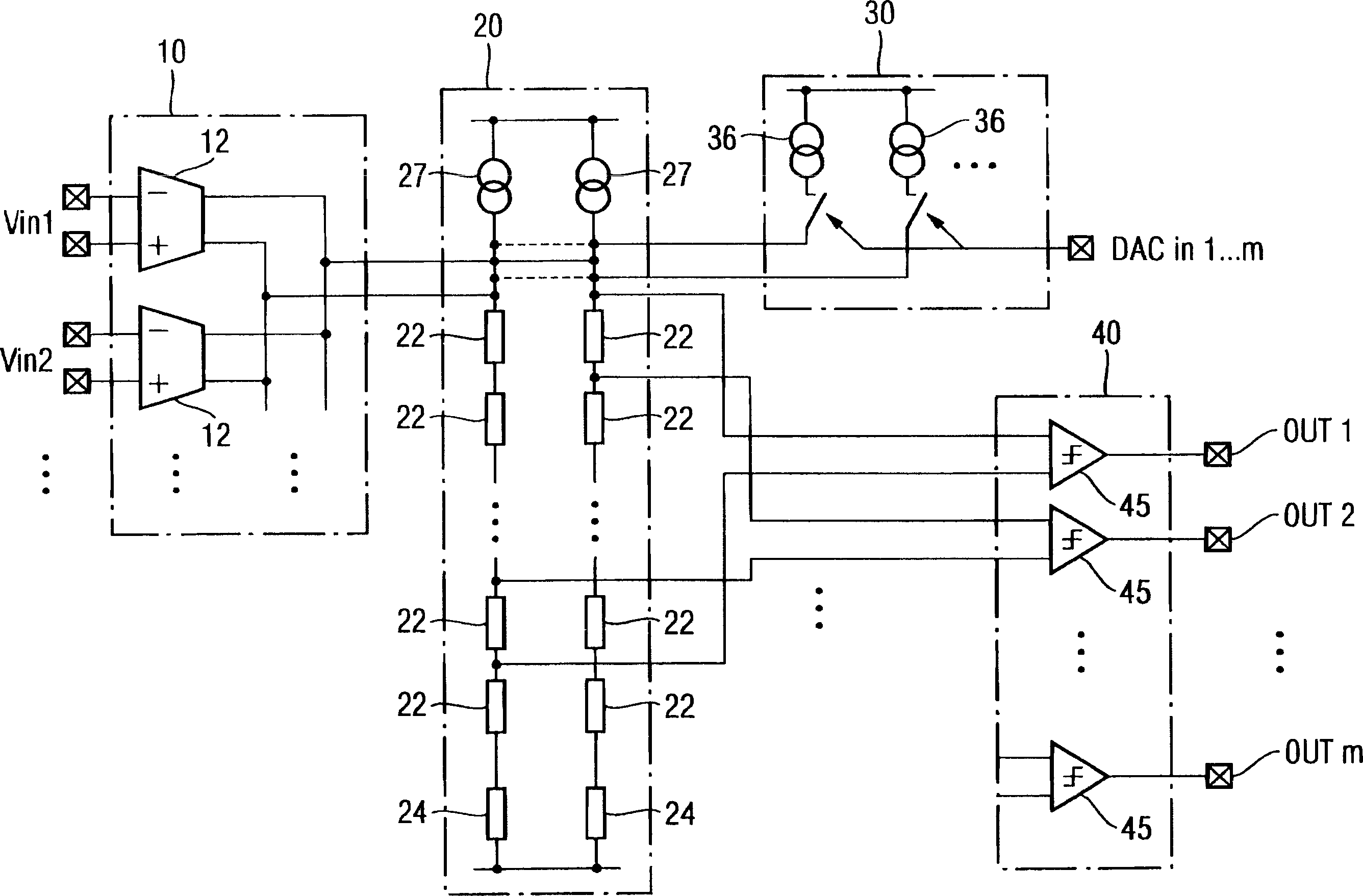
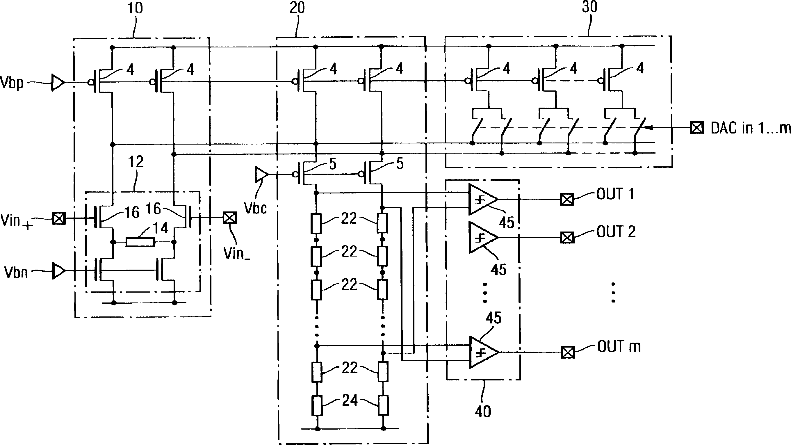
[0024] FIG. 1 schematically shows the circuit structure of a semiconductor circuit device according to an embodiment of the present invention. The semiconductor circuit device is configured for an inner loop of a ΣΔ modulator circuit, and includes an adding circuit 20 , a quantization circuit 40 , a digital-to-analog conversion circuit 30 and a voltage-current conversion circuit 10 .

[0025] The digital-to-analog conversion circuit 30 can convert the digital input signals DACin1 , . . . DACinm into current signals supplied to the addition circuit 20 . The digital-to-analog conversion circuit 30 is configured as a digital-to-analog conversion circuit based on parallel currents including m number of unit cells 36 . Each unit cell 36 includes a current source device that can provide a specific direct current, and it depends on the digital input signal being conducted to the first, positive output of the differential current output of the digital-to-analog conversion circuit 30, ...


PUM


Abstract

A semi-conductor circuit arrangement for a continuous time sigma delta modulator for adding analog input signals to a digital fed back signal and for quantizing the totalled signal comprises a voltage to current conversion circuit ( 10 ), an adding circuit ( 20 ) with a resistor ladder, a quantizing circuit ( 40 ) with comparator elements ( 45 ) and a digital to analog conversion circuit ( 30 ). For each comparator element ( 45 ) its respective input signal is formed by a voltage which is released between a tap in front of a corresponding tapping resistor ( 22 ) in a first string of the resistor ladder and a tap in front of a corresponding tapping resistor ( 22 ) in a second string of the resistor ladder.

Description

technical field [0001] The present invention relates to a semiconductor circuit device, especially a semiconductor circuit device for a continuous-time ΣΔ (sigmadelta) modulator circuit, such as a high-speed broadband transceiver. Background technique [0002] As a continuous time modulator, the ΣΔ modulator, commonly known as a continuous time ΣΔ modulator (CT-SD modulator), has a power consumption that is lower than that of a ΣΔ modulator used as a discrete time modulator. The advantage of being low makes these components especially suitable for wireless signal transmission devices. Alternatively, there is the advantage of higher bandwidth for signal processing at the same power consumption. Therefore, the use of ΣΔ modulators is particularly advantageous in high-speed broadband signal transmission such as VDSL-AFE transceivers. [0003] As shown in FIG. 3 , in the ΣΔ modulator circuit, the digital output signal 2 of the circuit is fed back to the analog input signal 1 t...

Claims


Application Information

Patent Timeline
IPC IPC(8): G06F7/50H03M1/12H03M1/74H03M3/00H03M3/02H03M3/04
CPCH03M3/454H03M3/452H03M3/39H03M3/424
Inventor M·克拉拉A·迪吉安多梅尼科A·维斯鲍尔
Owner INTEL CORP
Why Eureka
Try Eureka