Cutting device and method

A technology of cutting device and predetermined position, applied in capacitor manufacturing, electrical components, fixed capacitor dielectric, etc., can solve problems such as low processing speed, waste of time, cutting device cannot detect time, etc., achieve high-speed processing and improve work efficiency Effect

Active Publication Date: 2005-03-23
MURATA MFG CO LTD
View PDF1 Cites 15 Cited by
  • Summary
  • Abstract
  • Description
  • Claims
  • Application Information

AI Technical Summary

Problems solved by technology

[0006] However, the structure of the existing cutting device cannot detect this moment, so after confirming that the cutting tool has reached the highest position of the up and down movement, the positioning mark detection operation is started.
Therefore, there is a problem that time is unnecessarily wasted when switching from the cutting operation to the positioning mark detection operation.
[0007] In addition, because the structure of the conventional cutting device cannot det

Method used


Image

  • Cutting device and method
  • Cutting device and method
  • Cutting device and method

Examples


Embodiment

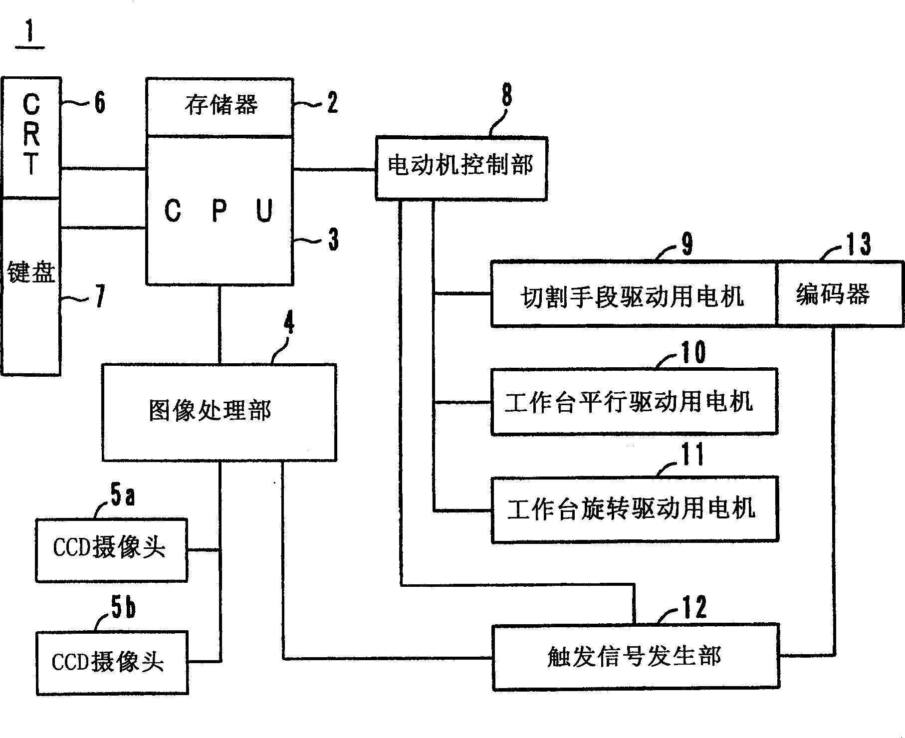
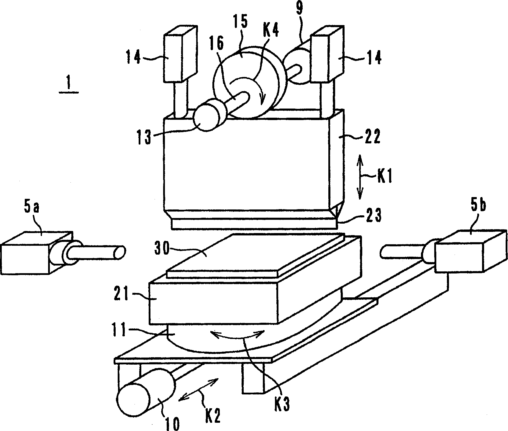
[0044] [Device outline configuration, figure 1 , figure 2 ]

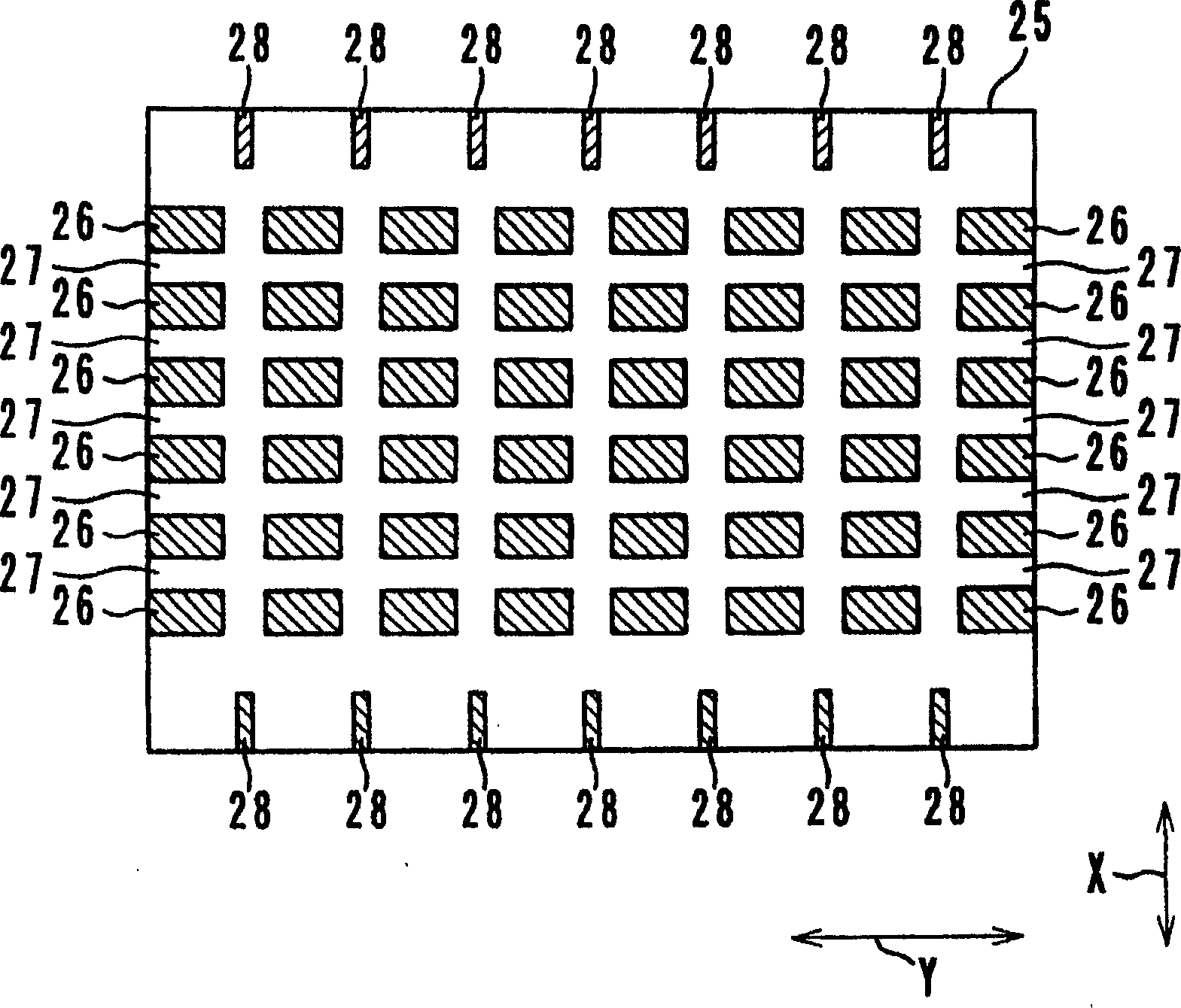
[0045] The manufacture of laminated ceramic capacitors usually goes through the following processes in sequence, including laminating multiple ceramic raw material substrates with multiple internal electrodes on the surface, and pressurizing them to form unsintered ceramic laminated blocks; The process of cutting the ceramic laminated block according to the configuration of the internal electrodes and cutting it into pieces of laminated ceramic chips; the process of sintering the cut laminated ceramic chips; and the process of forming external electrodes on the sintered laminated ceramic chips.

[0046] In this example, the cutting process adopts the system configuration shown in figure 1 , while the mechanical composition is shown in figure 2 The cutting device 1 to carry out. Cutting device 1 is made up of memory 2, computing unit (CPU) 3, image processing unit 4, CCD camera 5a, 5b, display unit (displays su...


PUM


Abstract

When a disk-like cam 15 rotates by 180[deg.], a cutting blade 23 reaches the lowest point and cuts a ceramic laminated block 30. When a motor 9 for driving cutting means rotates, the cutting blade 23 is changed from fall to rise. When an edge of the cutting blade 23 is exposed from the ceramic laminated block 30, a trigger signal is transmitted from a trigger signal generating part to an image processing part. When the image processing part receives the trigger signal, both end faces of the ceramic laminated block 30 are picked up by CCD cameras 5a, 5b, respectively, and a picked-up image for detecting a cut predetermined position is obtained. During the period, the cutting blade 23 continues to rise.

Description

technical field [0001] The invention relates to a cutting device and a cutting method. Background technique [0002] The manufacture of laminated ceramic electronic components such as laminated ceramic capacitors undergoes the following steps in sequence, including the process of printing multiple internal electrodes on the surface of the ceramic raw material substrate; The process of pressurizing and forming unsintered ceramic laminate blocks; the process of cutting the ceramic laminate blocks according to the configuration of the internal electrodes and cutting off the laminated ceramic chips one by one; the process of sintering the cut laminated ceramic chips process; and a process of forming external electrodes on the sintered laminated ceramic chip. [0003] However, in order to cut the ceramic laminate block at predetermined positions into laminated ceramic chips, printing marks for cutting and positioning are also printed in the process of printing a plurality of int...

Claims


Application Information

Patent Timeline
IPC IPC(8): B26D5/34B26D1/10B26D5/08B26D5/20B26D7/26H01G4/12H01G4/30H01G13/00
CPCB26D1/04H01G4/30H01L21/64
Inventor 山本良巳
Owner MURATA MFG CO LTD
Why Eureka
Try Eureka