
Producing method and structure for dynamic random access storage

A technology of dynamic random access and manufacturing method, applied in semiconductor/solid-state device manufacturing, electrical components, transistors, etc., can solve the problem of increasing junction leakage current, increasing the electric field gradient of PN junction, and inability to effectively reduce the total leakage current, etc. question

Inactive Publication Date: 2005-04-27
PROMOS TECH INC
View PDF1 Cites 1 Cited by
  • Summary
  • Abstract
  • Description
  • Claims
  • Application Information

AI Technical Summary

Problems solved by technology

However, this method will increase the electric field gradient of the PN junction, resulting in an increase in the junction leakage current, so the total leakage cannot be effectively reduced

Method used


Image

  • Producing method and structure for dynamic random access storage
  • Producing method and structure for dynamic random access storage
  • Producing method and structure for dynamic random access storage

Examples


Embodiment Construction

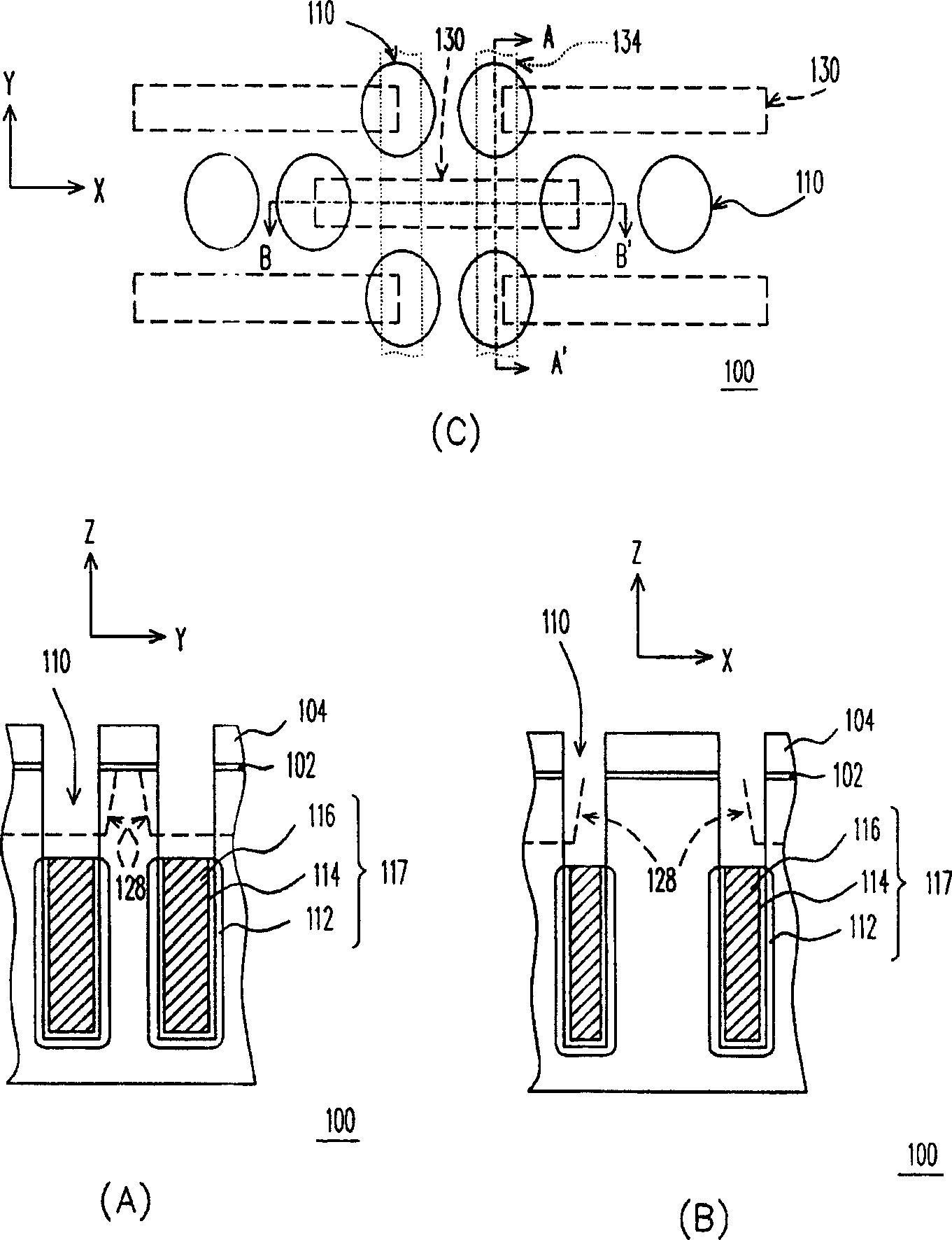
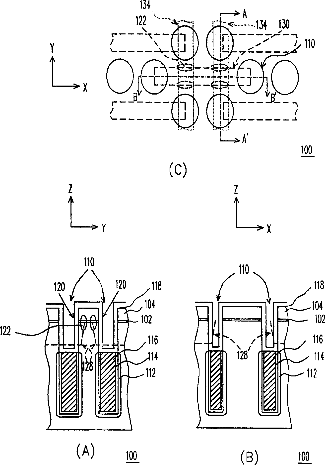
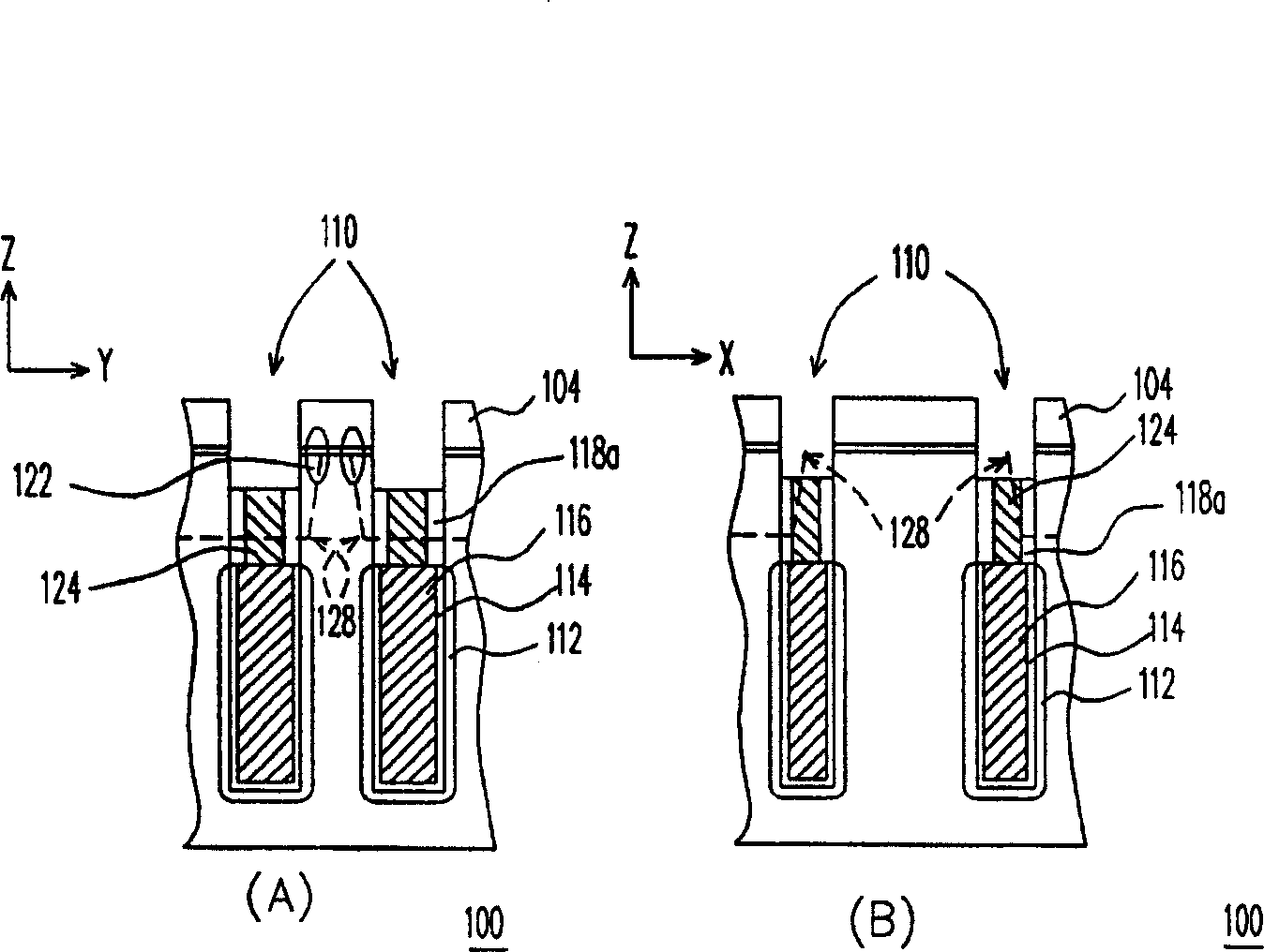
[0026] Please refer to Figures 1 to 8 , which show a method of manufacturing a dynamic random access memory according to a preferred embodiment of the present invention, wherein figure 1 , 2 The drawings in (C) in the icons in , 7 are respectively upper views, and the icons (A) / (B) are respectively the sectional views cut along the corresponding section line A-A' / B-B' in the corresponding figure (C).

[0027] Please refer to figure 1 In (A) / (B) / (C) diagrams, a substrate 100 is first provided, such as a P-type monocrystalline silicon substrate, and then a pad oxide layer 102 and a hard mask layer 104 are formed thereon, the hard mask The material of layer 104 is, for example, silicon nitride. Next, the hard mask layer 104 , the pad oxide layer 102 and the substrate 100 are sequentially defined to form a plurality of trenches 110 in the substrate 100 . These ditches 110 are arranged in accordance with 8F 2 Rules for eight F-square folded bit line DRAM layout, as disclosed...


PUM


Abstract

The present invention discloses the manufacture process and structure of DRAM with trench type capacitor. The DRAM manufacturing process includes forming a doped area with the same doping status with the substrate in the channel area part adjacent to the isolating area, and the doped area is formed through inclined ion implantation. The step of the inclined ion implantation is after forming capacitor trench and before defining active area. The doped area passes through the upper section of capacitor trench adjacent to the channel area and is implanted into the substrate in self-aligning mode.

Description

technical field [0001] The invention relates to a semiconductor manufacturing method, in particular to a dynamic random access memory manufacturing method. Background technique [0002] Dynamic Random Access Memory (DRAM) is a volatile memory used to store frequently accessed data in a computer. A typical DRAM cell is composed of a MOS transistor and a capacitor, wherein two sources / drains of the transistor are electrically connected to the capacitor and the bit line respectively. There are mainly two types of capacitors used in the current DRAM, one is a stacked capacitor that is higher than the transistor, and the other is a trench capacitor that is lower than the transistor. [0003] In a DRAM using a trench capacitor, in order to reduce the sub-threshold current of the transistor and increase the data storage capacity of the storage electrode, the initial voltage is often increased to adjust the ion implantation (V T implantation) and / or pocket ion implantation (pocke...

Claims


Application Information

Patent Timeline
IPC IPC(8): H01L21/8242H01L27/108
Inventor 李岳川陈赐龙
Owner PROMOS TECH INC
Learn More