Micron level chip packing structure

A chip packaging structure, micron-level technology, applied in electrical components, electrical solid-state devices, circuits, etc., can solve the problems of affecting the performance of the chip, reducing the bonding force of the ball joint, and reducing the stability.

Active Publication Date: 2005-04-27
JIANGYIN CHANGDIAN ADVANCED PACKAGING CO LTD
View PDF0 Cites 0 Cited by
  • Summary
  • Abstract
  • Description
  • Claims
  • Application Information

AI Technical Summary

Problems solved by technology

Since the solder ball is a wettable metal, when the solder ball is placed on the top of the metal layer, the metal layer will be covered by the solder ball and Cu will form after reflow. 3 Sn and Cu 6 sn 5 , so that the bonding force of the ball-planting joint is reduced, the stability is reduced, and the solder ball is easy to deviate from the pad, which affects the performance of the chip

Method used


Image

  • Micron level chip packing structure
  • Micron level chip packing structure
  • Micron level chip packing structure

Examples


Embodiment 1

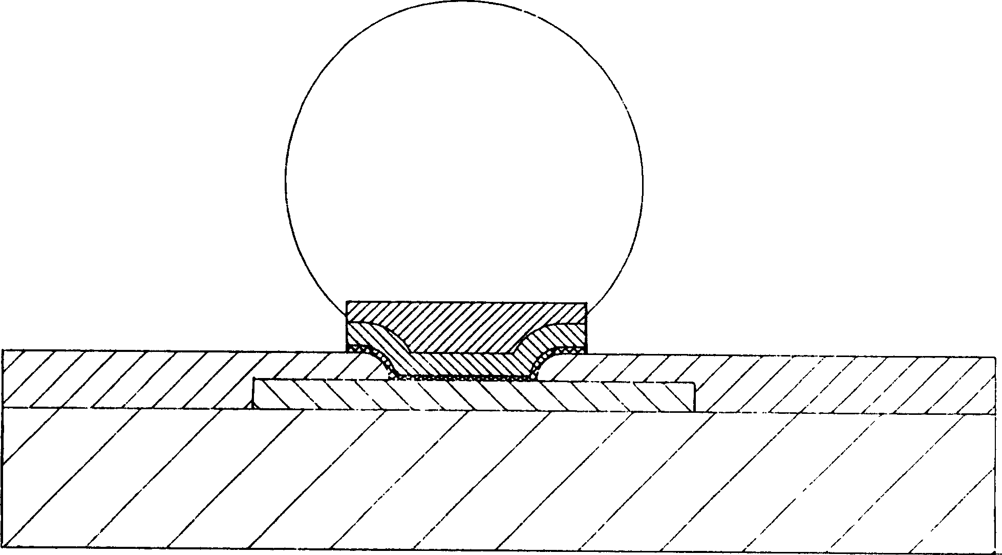
[0014] see figure 1 , the present invention is a micron-scale chip packaging structure, which is provided with a welding pad 2 on one surface of the chip body 1, the outer periphery of the welding pad 2 and the surface of the chip body 1 outside the outer periphery are provided with a protective layer 3, the surface of the welding pad 2 and A titanium layer 4, a copper layer 5 and a copper pillar 6 are sequentially superimposed on the protective layer 3 on the outer periphery, and solder balls 7 are planted on the top of the copper pillar 6, and all the solder balls are placed on the top of the copper pillar.

[0015] The thickness of the copper pillar 6 should be determined according to the reliability requirements of the chip, and is generally controlled within 5 μm˜100 μm.

Embodiment 2

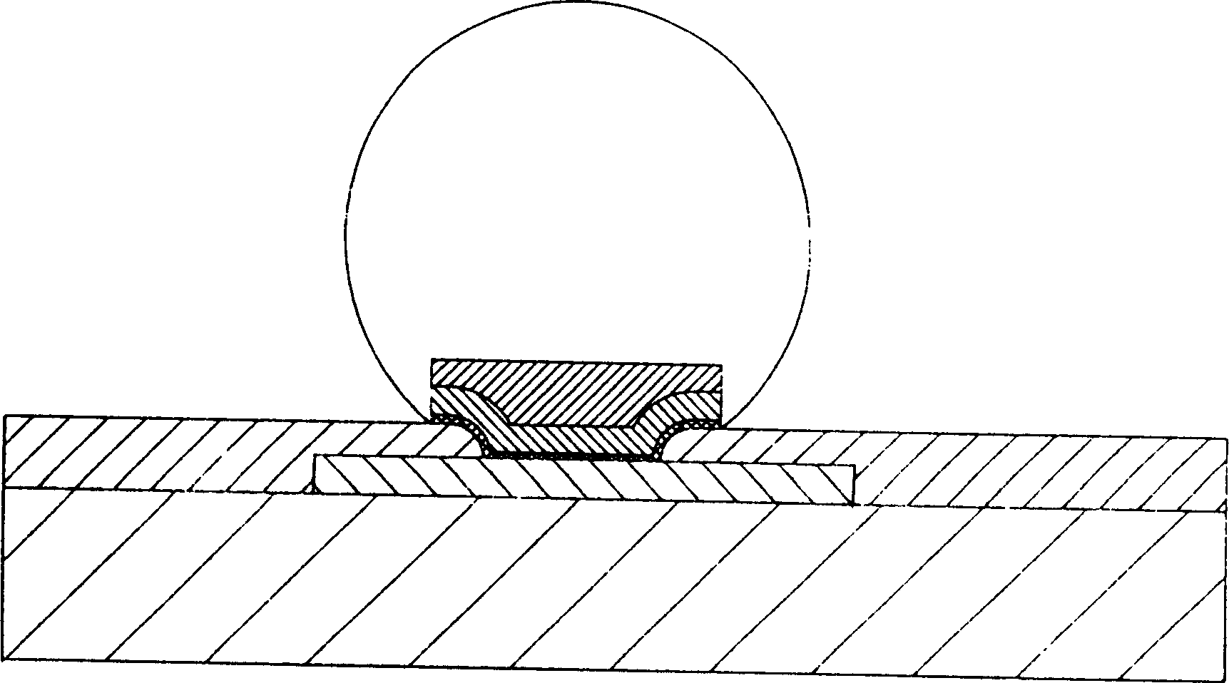
[0017] see figure 2 , the difference between this embodiment and the first embodiment is only that the solder balls 7 partially cover the copper pillars 6 .

Embodiment 3

[0019] see image 3 The only difference between this embodiment and the first embodiment is that the solder balls 7 completely cover the copper pillars 6 , the copper layer 5 and the titanium layer 4 .


PUM


Abstract

The present invention relates to one kind of micron level chip package structure. The chip package structure has chip body, soldering pad on the surface of the chip, protecting layer around the pad and on the surface of the chip body. It features that on the protecting layer, there are superposed titanium layer, copper layer, copper pin and tin ball successively. The package structure has raised ball planting binding force and certain space to avoid tin ball deviation from the soldering pad.

Description

Technical field: [0001] The invention relates to a micron-level chip packaging structure. It belongs to the technical field of packaging of integrated circuits or discrete devices. Background technique: [0002] In recent years, the demand for integrated circuit or discrete device consumer products has increased significantly, and their variety has increased accordingly. The reduction of metal wires in wafer fabs and the miniaturization of chip packaging products without affecting the performance and reliability of products are important pillars to meet such demands. [0003] Over the years, chip die packaging has been widely used, which is the smallest form factor package with almost no packaging or protective materials. This type of packaging usually refers to wafer-level chip packaging. The package area is as large as the chip area. The packaging structure is that a pad is provided on one surface of the chip body, a protective layer is provided on the outer periphery ...

Claims


Application Information

Patent Timeline
Patent Type & Authority Applications(China)
IPC IPC(8): H01L23/48
CPCH01L2224/10
Inventor 王新潮赖志明
Owner JIANGYIN CHANGDIAN ADVANCED PACKAGING CO LTD
Why Eureka
Try Eureka