Method and apparatus for measuring stress in semiconductor wafers

A technology of wafer and overall measurement, applied in the direction of measuring device, measuring force, adopting optical device, etc., can solve the problems of reduced reliability and reduced output

Inactive Publication Date: 2005-05-18
TEVET PROCESS CONTROL TECH
View PDF0 Cites 16 Cited by
  • Summary
  • Abstract
  • Description
  • Claims
  • Application Information

AI Technical Summary

Problems solved by technology

This stress can cause wafer bowing and cause cracks, voids, hillock forma

Method used


Image

  • Method and apparatus for measuring stress in semiconductor wafers
  • Method and apparatus for measuring stress in semiconductor wafers
  • Method and apparatus for measuring stress in semiconductor wafers

Examples


Embodiment Construction

[0139] Description of preferred embodiments

[0140] As an introduction to the present invention, the measurement method of PCT Patent Application No. WO0012958 is discussed in detail.

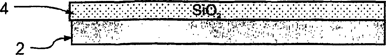
[0141] Reference is now made to FIG. 1A which shows a schematic cross-sectional view of a silicon wafer at an intermediate stage in the production process. Silicon wafer 2 has SiO attached to it 2 Layer 4. In Figure 1A the SiO 2 Layer 4 is homogeneous and only a single measurement is required to determine the layer thickness.

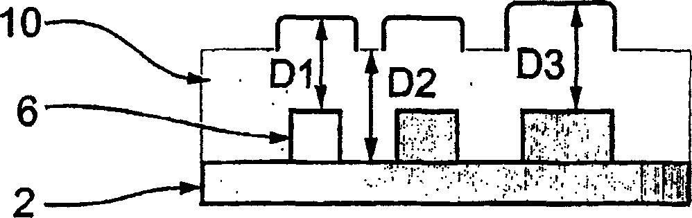
[0142] Reference is now made to FIG. 1B which shows a schematic cross-sectional view of another silicon wafer at another intermediate stage in the production process. In Figure 1B wafer 2 comprises a series of metal structures 6, and a continuous SiO 2 Layer 10. As will be explained in more detail below, the TMS measuring system is particularly suitable for measuring the thickness of transparent films. In this case, SiO 2 The layer 10 has thickness differences a...


PUM


Abstract

Integral measurement apparatus (50) and method for measuring layer thickness and bow in a wafer. The device comprises: a monochromatic light source (52), a white light source (100), a first switch (102) for switching between the white light source and the monochromatic light source, a switch for directing light from the switched light source to the semiconductor wafer A plurality of optical heads (56) at different locations on the surface (54), a first optical processor (104) for spectrally processing reflected light from the wafer, a second optical processor (104) for processing the reflected light to determine the degree of curvature in the wafer Two optical processors (58), and a second optical switch (106) for switching the reflected light from the wafer between the first optical processor and the second optical processor for spectral processing of white light to determine layer thickness , processes monochromatic light to determine the bend.

Description

field of invention [0001] The present invention relates to methods and apparatus for measuring stress in semiconductor wafers, and particularly, but not exclusively, to measuring stress and thickness in semiconductor wafers as a whole operation or apparatus. Background technique [0002] The semiconductor chip manufacturing process typically involves forming a silicon wafer and then performing a series of operations that primarily include adding and selectively removing layers to achieve chip functionality. [0003] Layer thickness and layer stress are two measurements performed on silicon wafers at various stages of the manufacturing process. In particular, in a semiconductor manufacturing process there are several steps in which a dielectric layer is deposited on a silicon wafer as part of the series mentioned above. [0004] After deposition, several properties of the layer are then tested to verify the quality of the layer itself and the quality of the deposition proces...

Claims


Application Information

Patent Timeline
IPC IPC(8): G01B11/00G01B11/06G01L1/00G01B11/16G01B11/24G01B11/30G01N3/06G01N3/20G01R31/265G01R31/28
CPCG01B11/16G01B11/245G01B11/306G01B2210/56G01R31/2656G01R31/2831H01L22/00
Inventor O·杜-诺尔Y·伊什-沙洛
Owner TEVET PROCESS CONTROL TECH
Why Eureka
Try Eureka