Method for forming metal-insulator-metal capacitance

A technology of metal capacitors and insulators, which is applied in the manufacture of circuits, electrical components, semiconductors/solid-state devices, etc.

Active Publication Date: 2005-06-08
SEMICON MFG INT (SHANGHAI) CORP +1
View PDF0 Cites 3 Cited by
  • Summary
  • Abstract
  • Description
  • Claims
  • Application Information

AI Technical Summary

Problems solved by technology

[0004] However, the problem with this known technology is that the parallel plate metal-insulator-metal capacitor manufacturing process will cause topography on the next layer of interconnection due to the additional top plate metal process.

Method used


Image

  • Method for forming metal-insulator-metal capacitance
  • Method for forming metal-insulator-metal capacitance
  • Method for forming metal-insulator-metal capacitance

Examples


Embodiment Construction

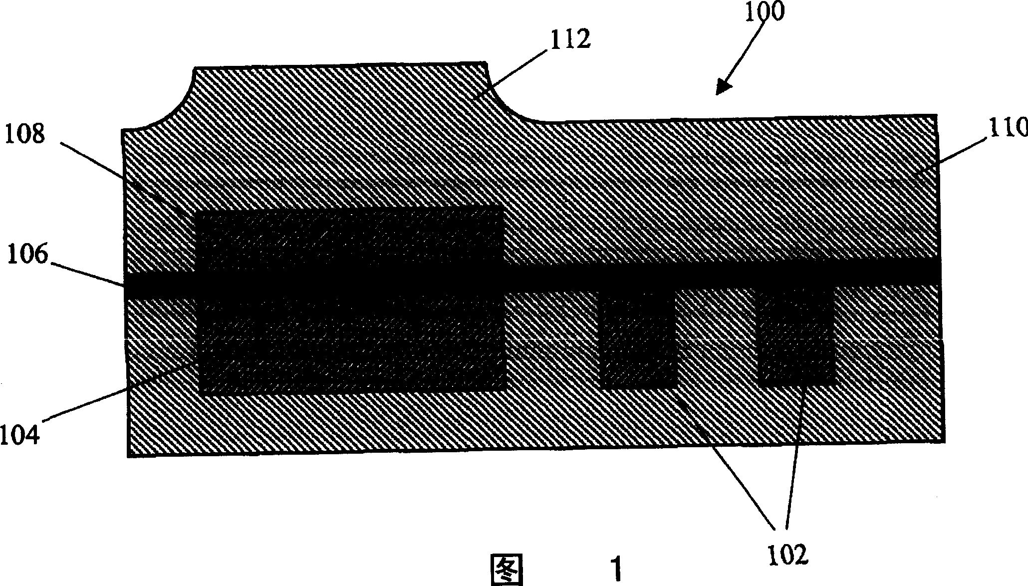
[0011] FIG. 1 shows a common parallel plate metal-insulator-metal capacitor structure 100 in the known art, wherein 102 represents the general copper wiring, 104 represents the copper bottom plate used as the lower plate of the capacitor, 106 represents the dielectric layer, and 108 represents The aluminum top plate, which acts as the upper plate of the capacitor, and 110 represent the interlayer dielectric. The process of this known technology requires cumbersome steps of barrier deposition, aluminum deposition, and aluminum patterning. In addition, due to the process of using the known technology, a surface topography (topography) 112 is inevitably created, which will make the damascene process of the next wiring layer more difficult to perform, and requires adding a chemical mechanical process before the patterning step. A polishing (CMP) step to planarize the surface of the dielectric layer.

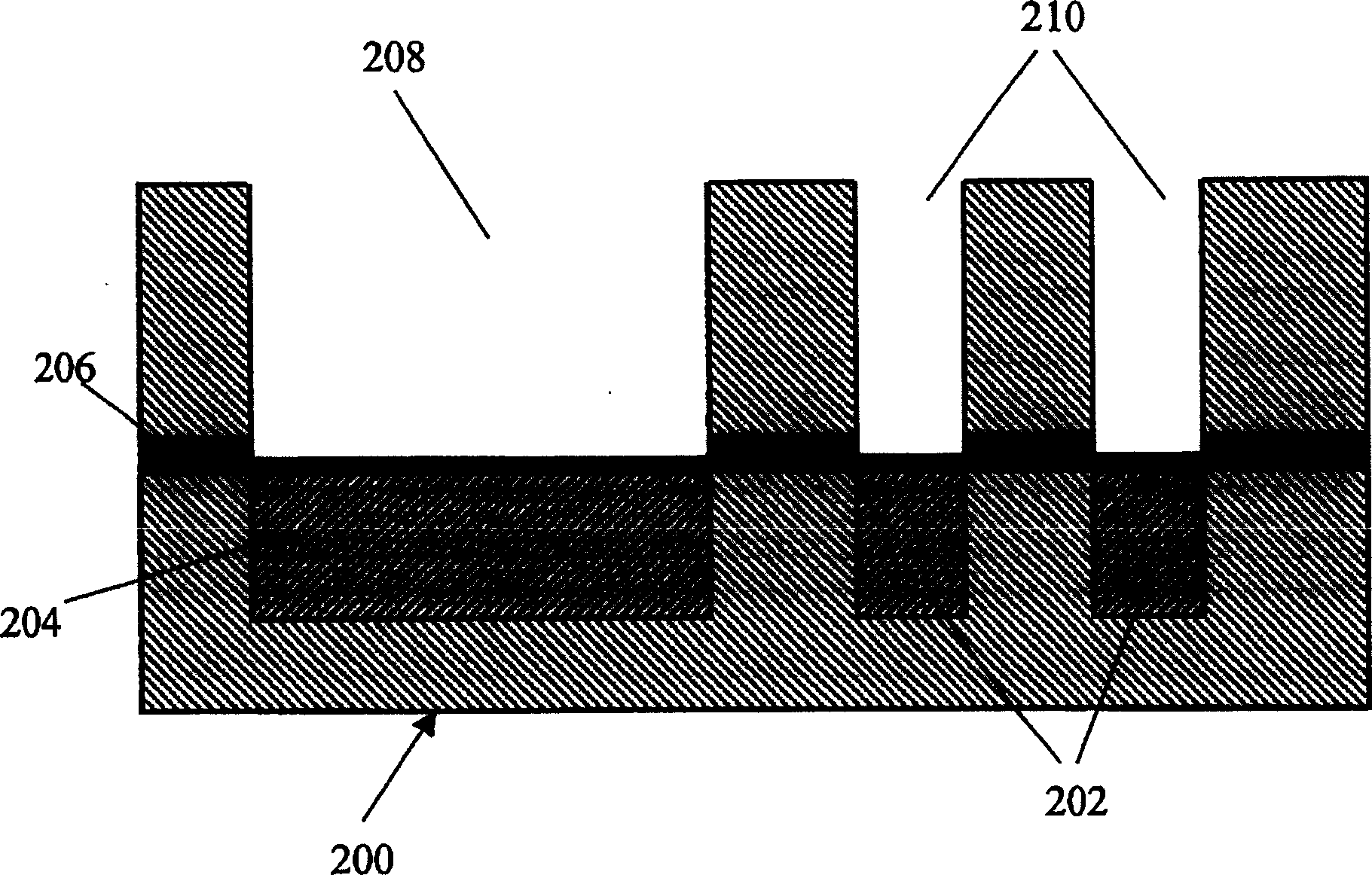
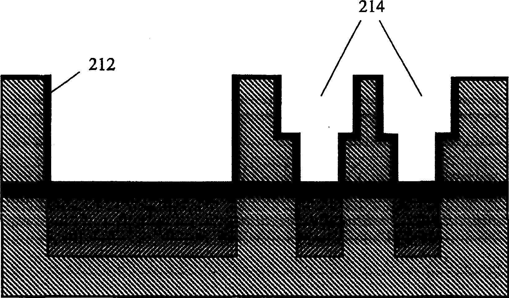
[0012] The following will refer to Figure 2 to Figure 6 To describe the method...


PUM

PropertyMeasurementUnit
thicknessaaaaaaaaaa
thicknessaaaaaaaaaa

Abstract

The invention discloses a method of forming the metal-insulation-metal capacitance on the base layer including dielectric layer, bronze bottom plate, bronze wire and blocking layer, the metal -insulation-metal capacitance is embedded in the bronze joint. This method includes the following processes: in the dielectric material on the blocking layer forms the through open hole with damascene structure and the placket on the flat plate of the metal-insulation-metal capacitance; deposit a dielectric layer on the relating placket, this dielectric layer is the middle insulation of the metal-insulation-metal capacitance; form a resist layer on the placket of the flat of the metal-insulation-metal capacitance; implement a photo etch procedure to eliminate the dielectric layer to unveil the bronze wiring, and the side wall of the through hole placket still has the dielectric layer to be as the metal block; then carry out the general bronze mutual connection technique (including metal block deposition, bronze crystal deposition, bronze electroplate, and chemical technological rubbing), so as to complete the metal-insulation-metal capacitance.

Description

technical field [0001] The present invention relates generally to semiconductor processing, and more particularly to methods of forming metal-insulator-metal (MIM) capacitors in copper damascene processing. Background technique [0002] With the advancement of semiconductor technology, the size of semiconductor devices is gradually shrinking. In order to shrink the size of semiconductor devices, the area occupied by features such as capacitors needs to be reduced. Therefore, a metal-insulator-metal (MIM) capacitor has been proposed in semiconductor technology. Metal-insulator-metal capacitors have been widely used in mixed-mode signaling devices and other applications. It is very cost-effective to embed metal-insulator-metal capacitors in copper interconnects. [0003] "SingleMask Metal-Insulator-metal (MIM) Capacitor with Copper DamasceneMetallization for sub-0.18μm Mixed Mode Signal and System-On- a-Chip (SoC) Applications" is an early technical document on the formati...

Claims


Application Information

Patent Timeline
Patent Type & Authority Applications(China)
IPC IPC(8): H01L21/70
Inventor 宁先捷
Owner SEMICON MFG INT (SHANGHAI) CORP
Why Eureka
Try Eureka