Semiconductor device

A technology of semiconductors and devices applied to the field of erroneous actions caused by erroneous signals

Inactive Publication Date: 2005-06-22
MITSUBISHI ELECTRIC CORP
View PDF2 Cites 14 Cited by
  • Summary
  • Abstract
  • Description
  • Claims
  • Application Information

AI Technical Summary

Problems solved by technology

[0013] The present invention is made to solve the above problems, and its object is to provide a semiconductor device capable of preventing erroneous operations caused by erroneous signals generated in the level shift circuit without affecting the normal operation of the level shift circuit.

Method used


Image

  • Semiconductor device
  • Semiconductor device
  • Semiconductor device

Examples


Embodiment 1

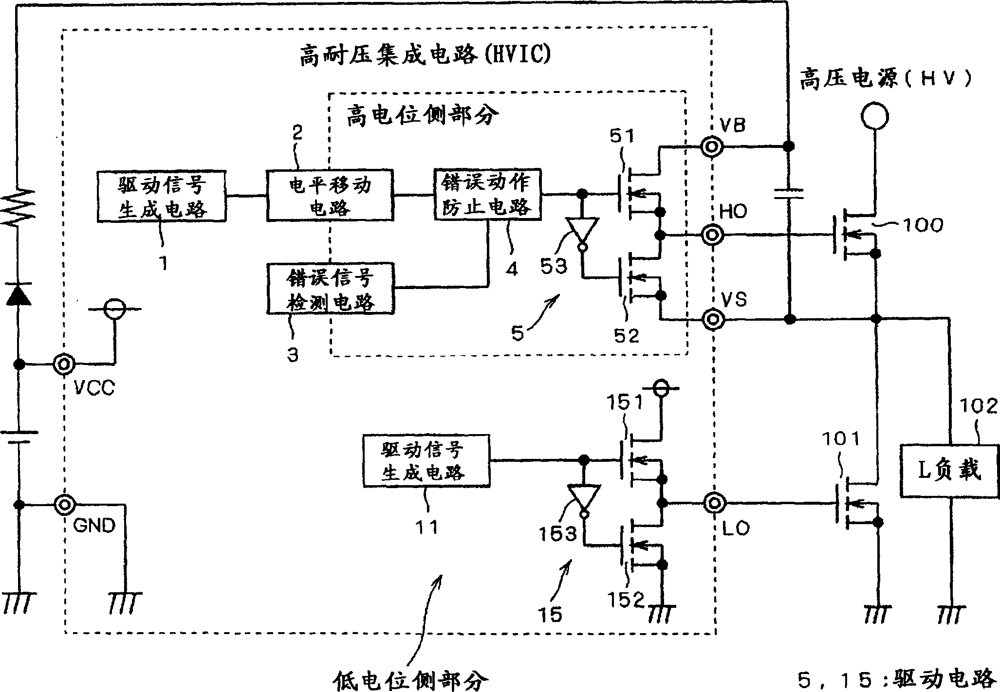
[0028] figure 1 It is a figure which shows the structure of the semiconductor device concerning Example 1, and shows the power device drive apparatus of the bootstrap system using the high withstand voltage integrated circuit (HVIC). In this semiconductor device, power semiconductor elements (MOSFET, IGBT, etc.) 100 and 101 connected in a half-bridge manner between a high-voltage power supply HV and GND are driven by an HVIC. An induction (L) load 102 such as a motor or a fluorescent lamp is connected to the power semiconductor element 101 of the lower arm.

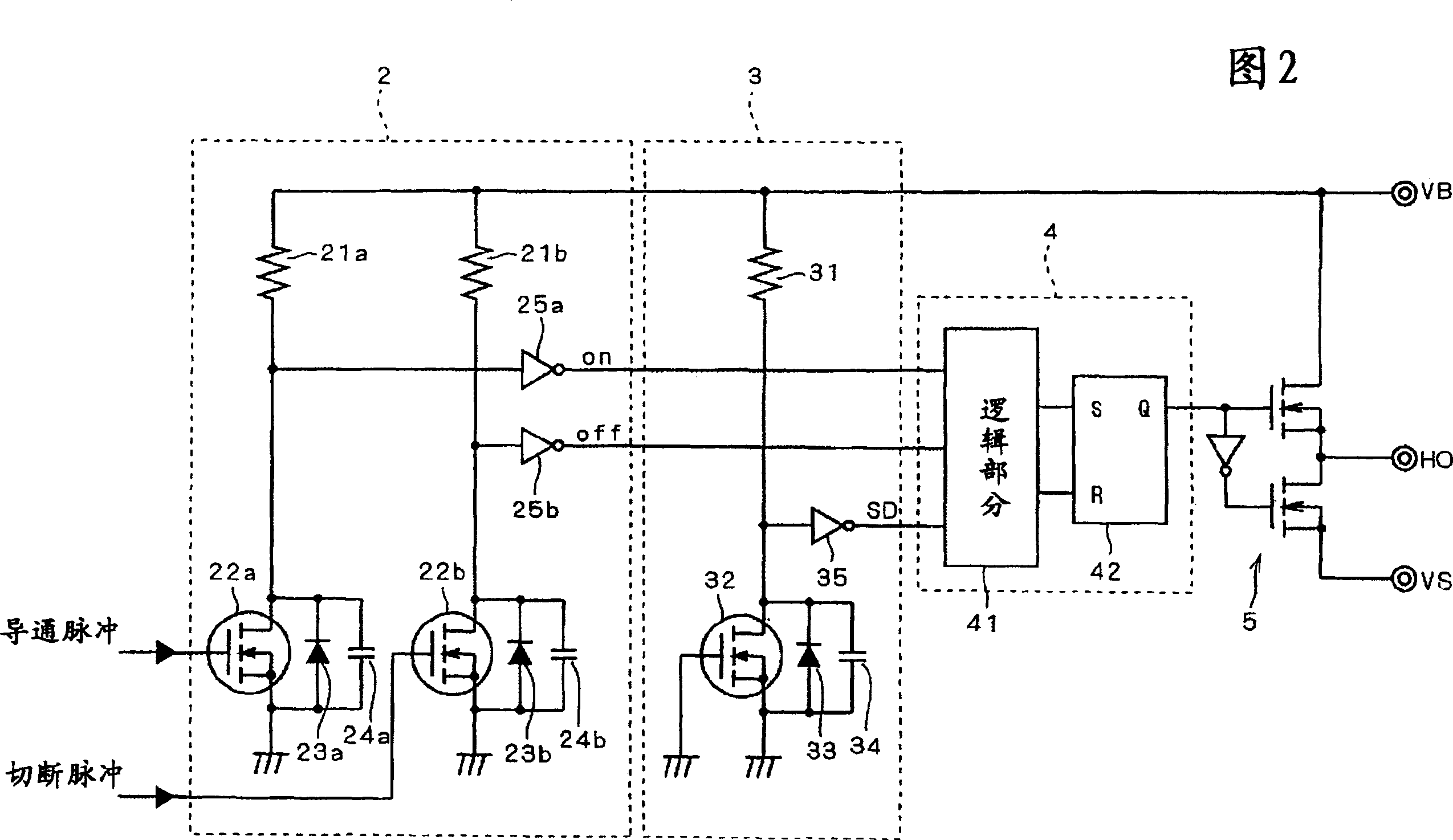
[0029] In this HVIC, the drive signal generating circuit 1 generates drive signals (on pulses and off pulses) as first signals for driving the power semiconductor element 100 of the upper arm. This drive signal is input to the level shift circuit unit 2, where it is converted (level shifted) into a second signal that can be transmitted to each circuit of the high potential side portion. The error signal detection circui...

Embodiment 2

[0048] Figure 4 A portion from the level shift circuit inside the HVIC to the output terminal on the high potential side in the semiconductor device related to Embodiment 2 is shown. This embodiment differs from Embodiment 1 only in the configuration of the error signal detection circuit 3, and the configuration of other elements and the overall operation of the semiconductor device are the same as those in Embodiment 1, so the description is omitted here.

[0049] like Figure 4 As shown, in the error signal detection circuit 3 of the second embodiment, the second switching element connected in parallel with the error signal detection resistor 31 is the diode element 36 connected in parallel with the capacitance element 37 . The anode of the diode element 36 is connected to the GND potential, and the cathode is connected to the high potential side power supply potential VB via the error signal detection resistor 31 . That is, the diode element 36 is fixed in the OFF state ...

Embodiment 3

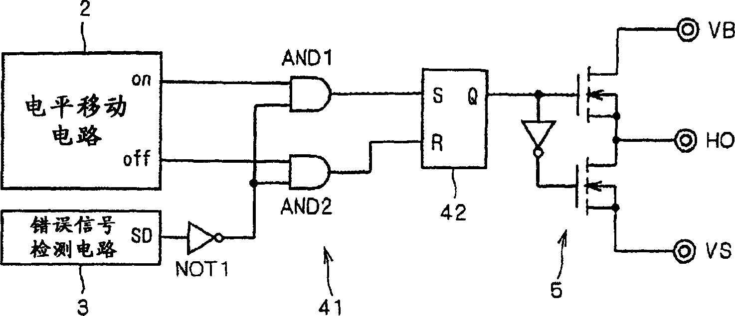
[0053] Figure 5 It is a diagram showing the structure of the malfunction prevention circuit 4 in the third embodiment. As shown in the figure, in this embodiment, the logic gates included in the logic section 41 of the malfunction prevention circuit 4 are AND3 and NOT2. The ON pulse from the level shift circuit 2 is input to one input terminal of AND3, and the OFF pulse is directly input to the R terminal of the RS flip-flop 42 . The error signal generation signal SD from the error signal detection circuit 3 is input to the other input terminal of AND3 through NOT2. Then, the output of AND3 is input to the S terminal of the RS flip-flop 42 .

[0054] Since the error signal generation signal SD is not input from the error signal detection circuit 3 (the error signal generation signal SD is low level) in the normal state where no error signal is generated in the level shift circuit 2, the input to the logic section 41 is The ON pulse and the OFF pulse are respectively input ...


PUM


Abstract

The semiconductor device of the present invention can prevent erroneous operation due to an erroneous signal generated in a level shift circuit. The error signal detection circuit (3) is connected in parallel with the level shift circuit (2), and the HVMOS (32) of the error signal detection circuit (3) is a dummy switching element fixed to an off state in a normal use state, It has the same structure as the two level shift circuits for on and off included in the level shift circuit (2). The voltage drop of the error signal detection resistor (31) is used as an error signal generation signal (SD) indicating the occurrence of an error signal in the level shift circuit (2), and is input to the error operation prevention circuit (4) through the NOT gate (35). )middle. A malfunction prevention circuit (4) performs predetermined malfunction prevention processing based on the malfunction signal generation signal (SD).

Description

technical field [0001] The present invention relates to a semiconductor device, and more particularly, to a technique for preventing erroneous operation caused by an erroneous signal generated in a level shift circuit. Background technique [0002] In a power semiconductor device (power semiconductor device), a power semiconductor element such as a MOSFET or an IGBT is driven by a high withstand voltage integrated circuit (hereinafter referred to as "HVIC"). For example, in the case of driving two power semiconductor elements such as the upper arm and the lower arm of a half-bridge type inverter, a power semiconductor element having a high-potential side (high-potential island) of the power semiconductor element driving the upper arm is used. A driver circuit and an HVIC that drives the driver circuit on the low-potential side (low-potential island) of the power semiconductor element of the lower arm. Such a HVIC includes a so-called level shift circuit that transmits a dri...

Claims


Application Information

Patent Timeline
Patent Type & Authority Applications(China)
IPC IPC(8): H01L27/04G06F11/00H01L21/822H02M1/08H03K17/0812H03K17/16H03K19/00H03K19/0175H03K19/0185
CPCH03K17/08122H03K17/162H03K19/00H03K19/0175
Inventor 折田昭一
Owner MITSUBISHI ELECTRIC CORP
Why Eureka
Try Eureka