Shallow junction shield groove technique for protecting active region area

A technology for isolating trenches and active areas, which is applied in the fields of electrical components, semiconductor/solid-state device manufacturing, circuits, etc., and can solve problems such as reducing the effective area of ​​the active area, affecting the high density of devices and CD control.

Inactive Publication Date: 2005-06-29
SHANGHAI HUA HONG GROUP +1
View PDF0 Cites 0 Cited by
  • Summary
  • Abstract
  • Description
  • Claims
  • Application Information

AI Technical Summary

Problems solved by technology

However, although such a pull-back process improves the corner shape of STI and makes it round, it inevitably reduces the effective area of ​​the active region. A retreat will seriously affect the high density and CD control of the device, especially for high density devices such as memory.

Method used


Image

  • Shallow junction shield groove technique for protecting active region area
  • Shallow junction shield groove technique for protecting active region area
  • Shallow junction shield groove technique for protecting active region area

Examples


Embodiment Construction

[0031] The present invention is in conventional STI process, reaches the above-mentioned object by the method for increasing a MASK and relevant process step, therefore, the main process step of process method of the present invention is listed below (particularly different from conventional STI process flow The process steps), that is, in the STI process flow, the process before the STI planarization, and the subsequent processes are consistent with the processes in other conventional STI processes, and will not be repeated here.

[0032] The following is the process steps before STI CMP in the process flow of this STI (see the description of the drawings):

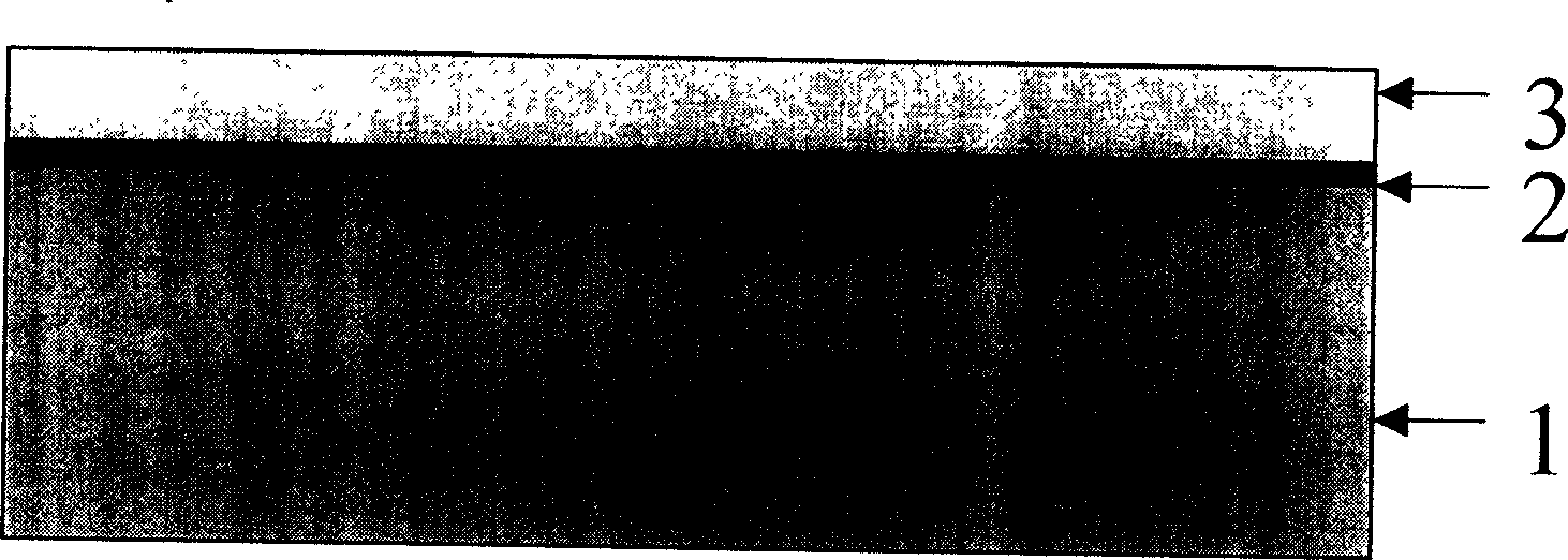
[0033] 1. Deposit silicon oxide and silicon nitride layers, as the HARD MASK defined by STI, the thicknesses are silicon oxide: 10nm; silicon nitride: 200nm; ( figure 1 )

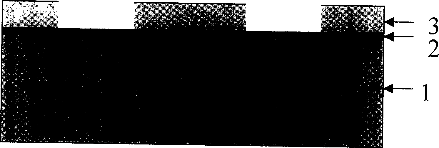
[0034] 2. Use STI MASK to define the STI and active area, that is, the photolithography process

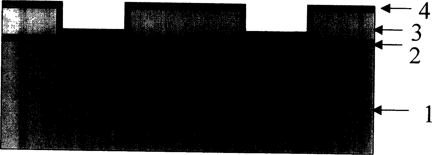
[0035] 3. Etching silicon oxide to expose the STI...


PUM


Abstract

This invention relates to a new STI process to protect the source area. With the integration degree rapidly increase, people integrates multiple circuits and devices in one chip. In order to ensure the core logic circuit high property and increases the capacity and density of the memory, this invention provides a new STI process to distinguish the high density silicon area and the silicon pad need to be improved.

Description

technical field [0001] The invention belongs to the technical field of integrated circuit technology, and in particular relates to a new STI technology for protecting the area of ​​an active region. Background technique [0002] In today's advanced semiconductor process technology, shallow junction isolation trench (STI) technology is the most important and most difficult process module in the front-end process. Although this module process has been widely used in the advanced semiconductor manufacturing process technology of 0.25 micron and below, its process method is also continuously improved and developed with the continuous upgrading of process technology. The basic technical requirement for STI is: when a large number of transistors and other devices are integrated into smaller and smaller chips, it can play a good role in insulating and isolating each tiny device without affecting these devices. device operating characteristics. In fact, when people carve fine STI ...

Claims


Application Information

Patent Timeline
Patent Type & Authority Applications(China)
IPC IPC(8): H01L21/76
Inventor 陈寿面杨左娅
Owner SHANGHAI HUA HONG GROUP
Why Eureka
Try Eureka