

Power semiconductor device
A power semiconductor and semiconductor technology, applied in semiconductor devices, transistors, electrical components, etc., can solve problems such as avalanche withstand capability without considering the characteristics of power devices, and achieve interface instability, high avalanche withstand capability, and low on-resistance. Effect
- Summary
- Abstract
- Description
- Claims
- Application Information
AI Technical Summary
Problems solved by technology
Method used
Image

Examples
no. 1 example
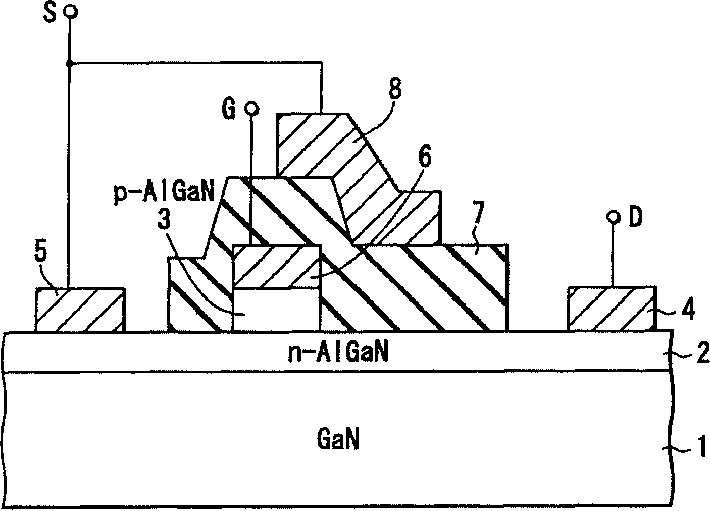
[0033] figure 1 is a cross-sectional view schematically showing the structure of a junction power HEMT (High Electron Mobility Transistor) according to a first embodiment of the present invention.
[0034] The HEMT is provided with a channel layer 1 comprising as undoped Al X Ga 1-X GaN layer (X=0) of N (0≤X≤1). The thickness of the channel layer 1 is set to be about 1 to 2 μm in order to obtain a breakdown voltage of 600V. On the surface (one side) of the channel layer 1 is formed as n-type Al Y Ga 1-Y The barrier layer 2 of N (0≤Y≤1, X0.2 Ga 0.8 N layer (Y=0.2), which is doped as an impurity with a dose of about 10 13 (atoms / cm 2 ) Si. Further, the semiconductor layer 3 is selectively formed on the barrier layer 2 as p-type Al Z Ga 1-Z N (0≤Z≤1), and its thickness is 0.01 μm. The semiconductor layer 3 includes Al in which Mg is doped as an impurity 0.1 Ga 0.9 N(Z=0.1).
[0035] A drain electrode (D: first electrode) 4 and a source electrode (S: second electrode...
no. 2 example
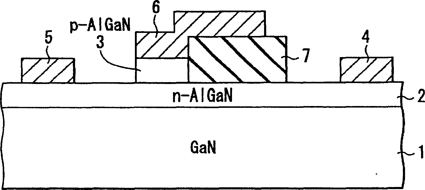
[0058] Figure 5 is a cross-sectional view schematically showing the structure of a junction power HEMT according to a second embodiment of the present invention. exist figure 1 In the power HEMT, the semiconductor layer 3 including the p-AlGaN layer is formed to have the same length as the gate electrode 6 . That is, the end of the semiconductor layer 3 on the side of the drain electrode 4 is positionally aligned with the end of the gate electrode 6 on the side of the drain electrode 4 .
[0059] In contrast, in the power HEMT of the second embodiment, the semiconductor layer 3 including the p-AlGaN layer is formed so that the end portion on the drain electrode 4 side can extend from the end portion of the gate electrode 6 on the drain electrode 4 side to the one side of the drain electrode 4 . Further, the semiconductor layer 3 is formed so that the end portion on the side of the drain electrode 4 can be located under the field plate electrode 8 .
[0060] Figure 6A is a...
no. 3 example
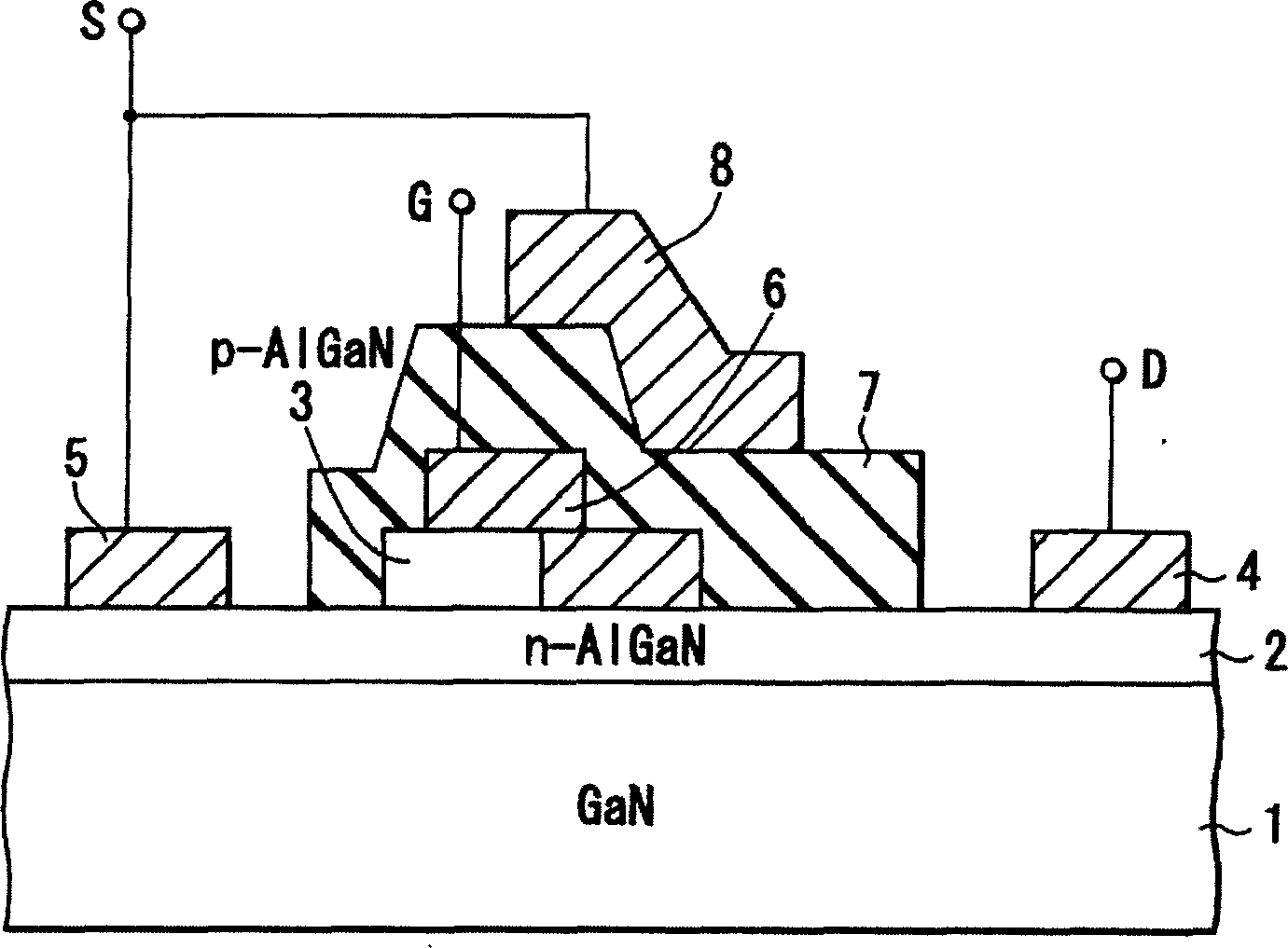
[0082] Figure 8 is a cross-sectional view showing the structure of a junction power HEMT according to a third embodiment of the present invention. The distance between gate and drain determines figure 1 The breakdown voltage of the lateral type power device shown; therefore, it is desirable to set the above distance to be longer. In addition, the distance between the source and the gate, which has nothing to do with the breakdown voltage, is shortened. This is useful for reducing on-resistance. In the power HEMT of the third embodiment, the distance between the gate and the drain is set wider than the distance between the gate and the source in order to achieve high breakdown voltage and low on-resistance. More specifically, the distance Lgd is set wider than the distance Lgs. That is, the distance Lgd is the length between the end of the gate electrode 6 on the side of the drain electrode 4 and the end of the drain electrode 4 on the side of the gate electrode 6 . The d...
PUM
 Abstract
Description
Claims
Application Information