
Active matrix panel

An active matrix and panel technology, applied in optics, instruments, electrical components, etc., can solve the problems of larger configuration space and smaller aperture ratio, reducing configuration space, increasing aperture ratio, and reducing pixel pitch. Effect

Active Publication Date: 2005-08-10
INTERDIGITAL CE PATENT HLDG
View PDF1 Cites 8 Cited by
  • Summary
  • Abstract
  • Description
  • Claims
  • Application Information

AI Technical Summary

Problems solved by technology

[0003] However, in the above-mentioned existing active matrix panel, since the two thin film transistors are only arranged in series in the vicinity of the intersections of the scan lines and the data lines arranged in a matrix in the lateral direction, the area occupied by the two thin film transistors in the lateral direction is The layout space becomes larger, which becomes an obstacle when the pixel pitch is reduced, or the aperture ratio becomes smaller.

Method used


Image

  • Active matrix panel
  • Active matrix panel
  • Active matrix panel

Examples


no. 1 Embodiment approach

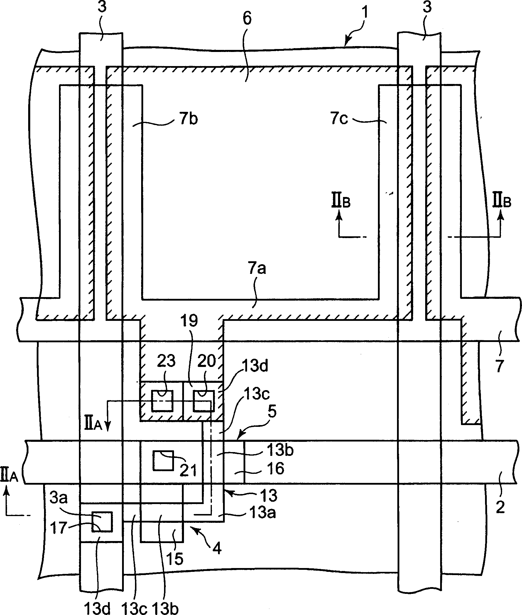
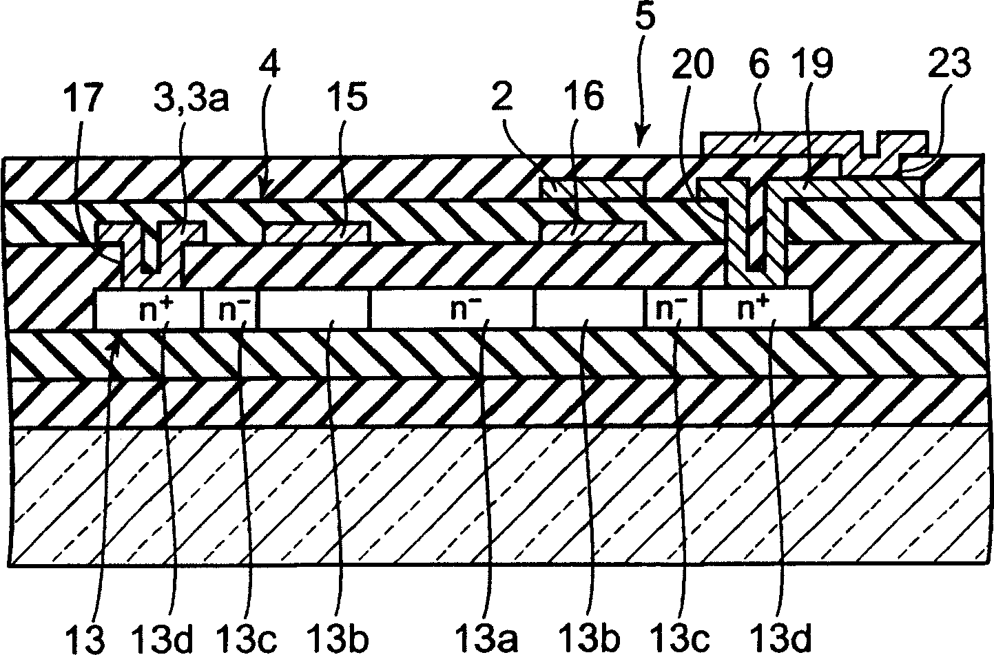
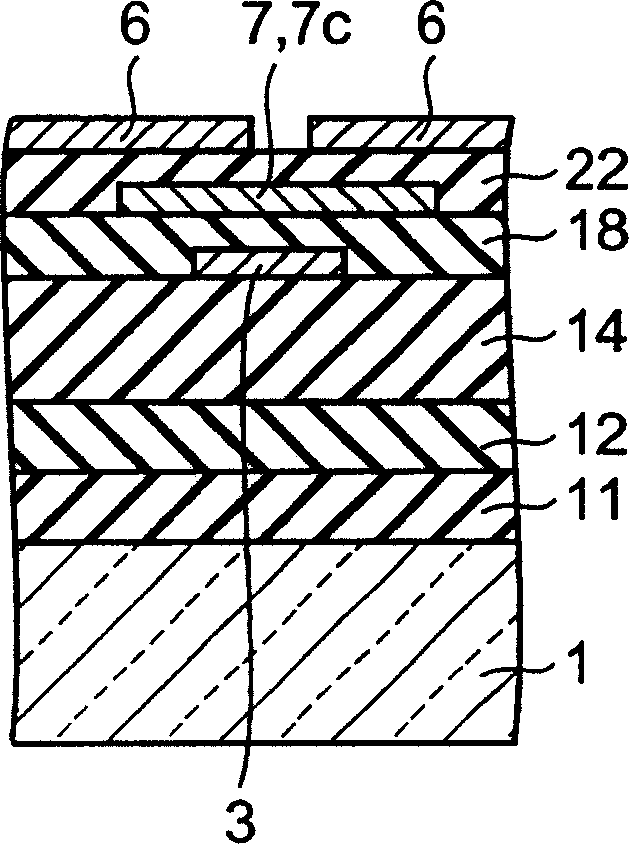
[0028] figure 1 It is a perspective plan view showing a main part of the active matrix panel of the liquid crystal display device according to the first embodiment of the present invention. The active matrix panel has a glass substrate 1 . Scanning lines 2 and data lines 3 are arranged in a matrix on one side of the upper surface of the glass substrate 1, and two thin film transistors (switching elements) 4, 5, pixel electrodes 6 and auxiliary electrodes connected in series are arranged near their intersections. Capacitive electrode 7. Here, in order to make figure 1 To be clear, the edge portion of each pixel electrode 6 is hatched with an oblique short solid line.

[0029] Edge portions on the left and right sides of the pixel electrode 6 coincide with the data lines 3 disposed on the left and right sides. exist figure 1 Among them, the auxiliary capacitor electrode 7 has: a linear electrode portion 7a arranged in parallel with the scanning line 2, a rectangular elec...

no. 2 Embodiment approach

[0054] Figure 9 A perspective plan view showing main parts of an active matrix panel of a liquid crystal display device according to a second embodiment of the present invention, Figure 10A is along Figure 9 the X A -X A cutaway view of the line, Figure 10B is along Figure 9 the X B -X B Cutaway view of the line. In addition, here in order to make Figure 9 To be clear, the edge portion of each pixel electrode 6 is hatched with a slanted short solid line.

[0055] Next, neutralize the active matrix panel figure 1 The difference from the situation shown in Fig. 2 will be described. One difference is that the interlayer insulating film 18 is omitted, and on the upper surface of the second underlying insulating film 12 including the upper surface of an n-type high-doped concentration region 13d of the semiconductor thin film 13, a data electrode 3a serving also as the drain electrode 3a is formed. Line 3 forms an island-shaped source on the upper surface of anoth...

no. 3 Embodiment approach

[0058] In each of the above-mentioned embodiments, the case where the present invention is applied to a coplanar type suitable as an active matrix panel having a semiconductor thin film transistor made of polysilicon has been described. However, the present invention is not limited thereto, and can also be applied to Inverse staggered type suitable for active matrix panels with semiconductor thin film transistors made of amorphous silicon.

[0059] Figure 11 A perspective plan view showing main parts of an active matrix panel of a liquid crystal display device according to a third embodiment of the present invention. The active matrix panel has a glass substrate 41 . Scanning lines 42 and data lines 43 are arranged in a matrix on the upper surface of the glass substrate 41 , and two thin film transistors 44 and 45 connected in series, pixel electrodes 46 and storage capacitor electrodes 47 are arranged near their intersections. Here, in order to make Figure 11 To be clear...


PUM


Abstract

The invention provides an active matrix panel, which comprises a plurality of scanning beams (2), a plurality of data lines (3), and a plurality of switch elements (4,5) separately connected with the scanning beams (2) and the data lines (3); the switch elements (4,5,44,45) separately comprises semiconductor films (13,54), gate insulating films (14,53) and gate electrodes (15,16,51,52). The lateral configuration space occupied by the two thin film transistors (TFT) can be reduced, thereupon, the pixels interval can be reduced, or the aperture ratio can be increased.

Description

technical field [0001] The present invention relates to active matrix panels. Background technique [0002] In an active matrix panel of a liquid crystal display device, thin-film transistors are provided near the intersections of scan lines and data lines arranged in a matrix and connected to two lines, and pixel electrodes are connected to each thin-film transistor. structure. In this active matrix panel, in order not to reduce the on-current of the thin film transistor, the off-current is greatly reduced, as shown in JP-A-58-171860 ( Image 6 As shown in (a)), for example, there is a structure in which two thin film transistors are arranged in series in the lateral direction near each intersection of scanning lines and data lines arranged in a matrix. [0003] However, in the above-mentioned existing active matrix panel, since the two thin film transistors are only arranged in series in the vicinity of the intersections of the scan lines and the data lines arranged in a ...

Claims


Application Information

Patent Timeline
Patent Type & Authority Applications(China)
IPC IPC(8): G02F1/1368G09F9/30H01L21/77H01L21/84H01L27/12H01L29/786
CPCH01L29/78645H01L29/78696H01L27/12H01L29/78621H01L27/1214H01L27/124B25H1/16
Inventor 中村弥生
Owner INTERDIGITAL CE PATENT HLDG
Learn More