Semiconductor memory device and method for making same

A technology for storage devices and manufacturing methods, which is applied in semiconductor/solid-state device manufacturing, semiconductor devices, information storage, etc., and can solve the problems of reducing the number of storage units and increasing the loss of transistor area

Inactive Publication Date: 2005-08-17
RENESAS TECH CORP
View PDF3 Cites 0 Cited by
  • Summary
  • Abstract
  • Description
  • Claims
  • Application Information

AI Technical Summary

Problems solved by technology

However, if a structure in which the local data line is connected to the global data line via a switch at a short distance is simply adopted, the number of memory cells per local data line decreases, and there is a problem that the area loss of the selection transistor portion increases.
In addition, especially with the advancement of miniaturization, the width of electrodes running parallel to the data lines is also required to be reduced. As a result, the wiring width of the inversion layer is also reduced, so the problem of resistance becomes significant.

Method used


Image

  • Semiconductor memory device and method for making same
  • Semiconductor memory device and method for making same
  • Semiconductor memory device and method for making same

Examples


Embodiment Construction

[0049] Hereinafter, embodiments of the present invention will be described in detail with reference to the drawings. In addition, throughout the drawings for describing the embodiments, the same members are given the same reference numerals in principle, and overlapping descriptions thereof will be omitted.

[0050] (Embodiment 1)

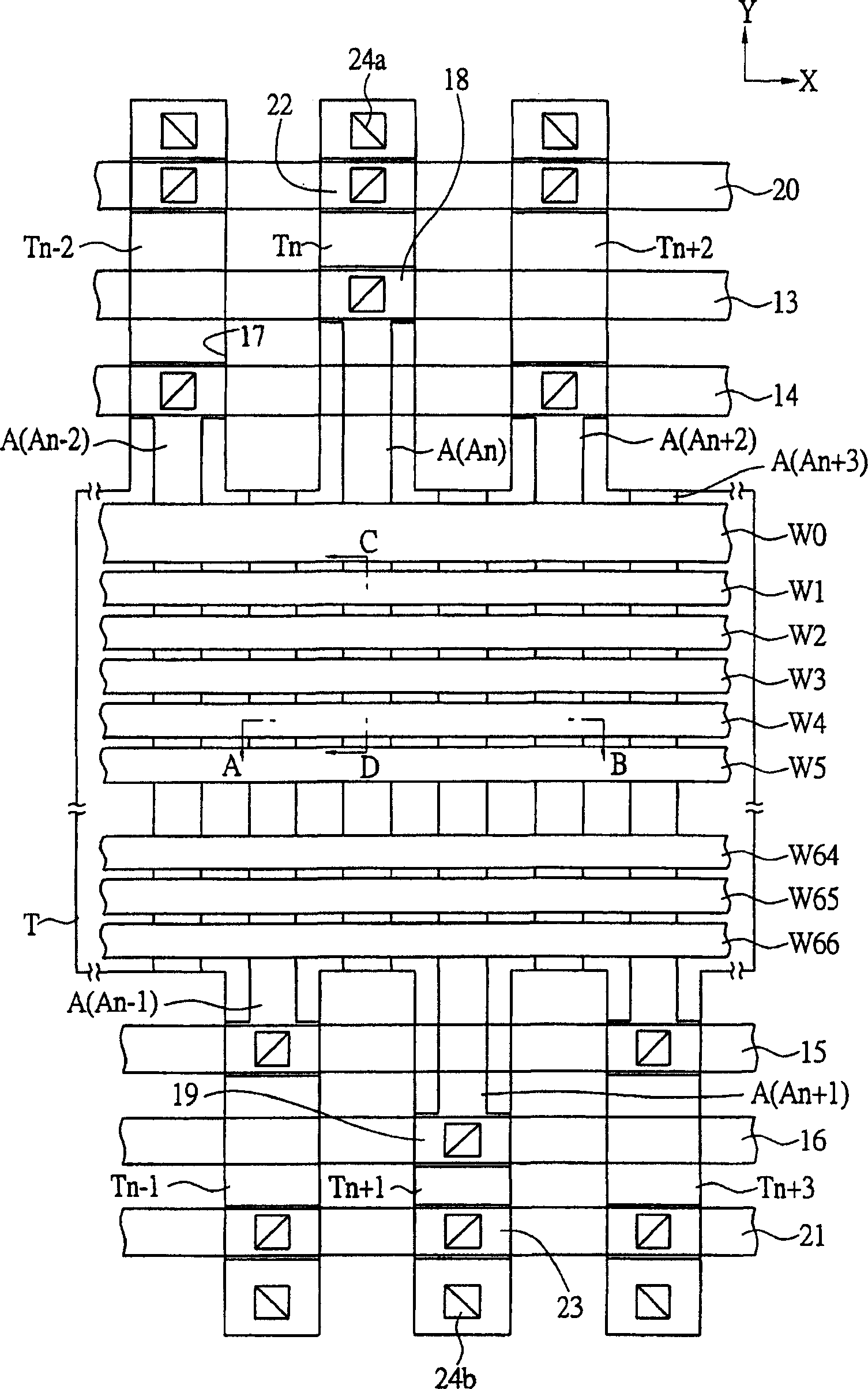
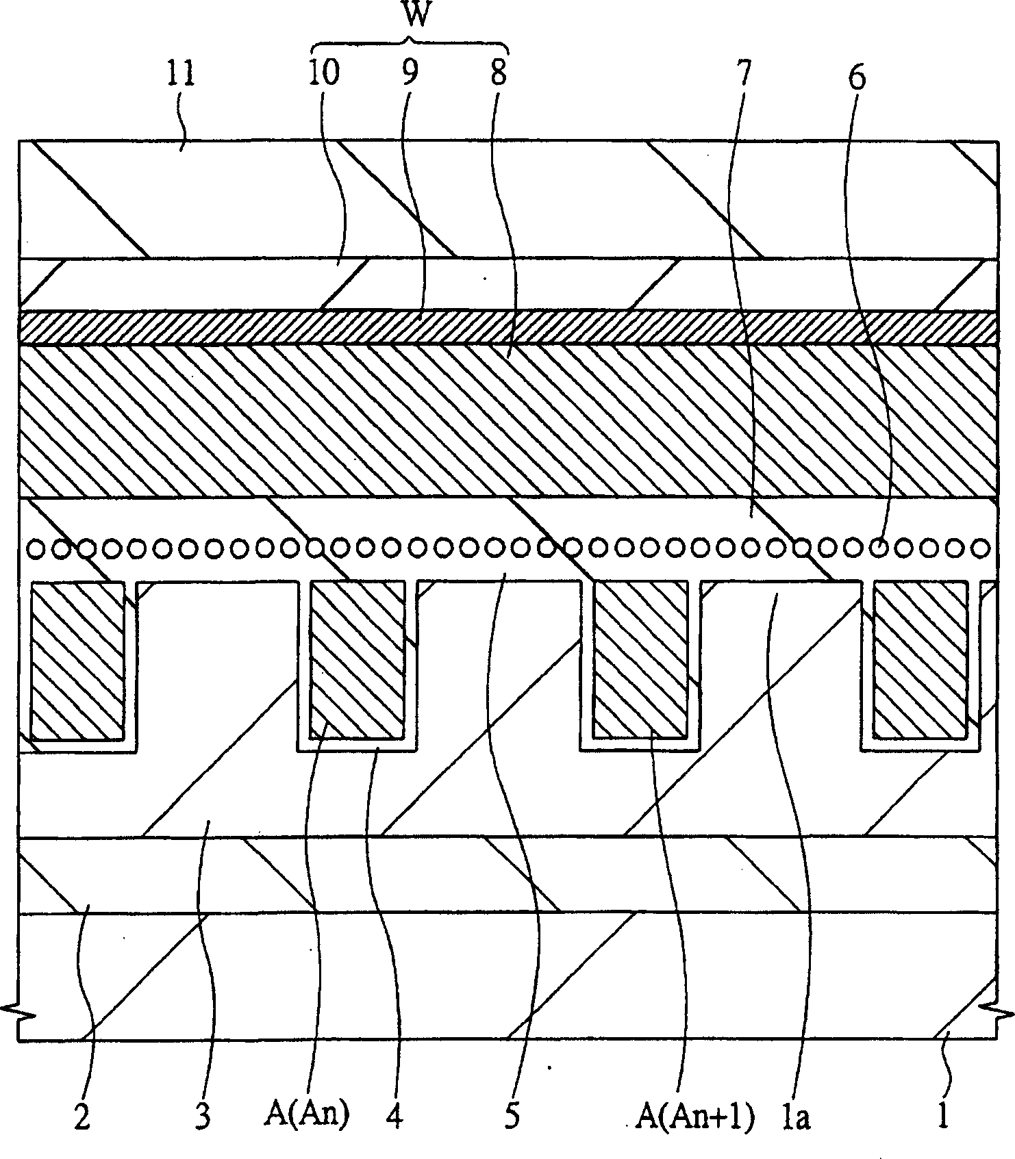
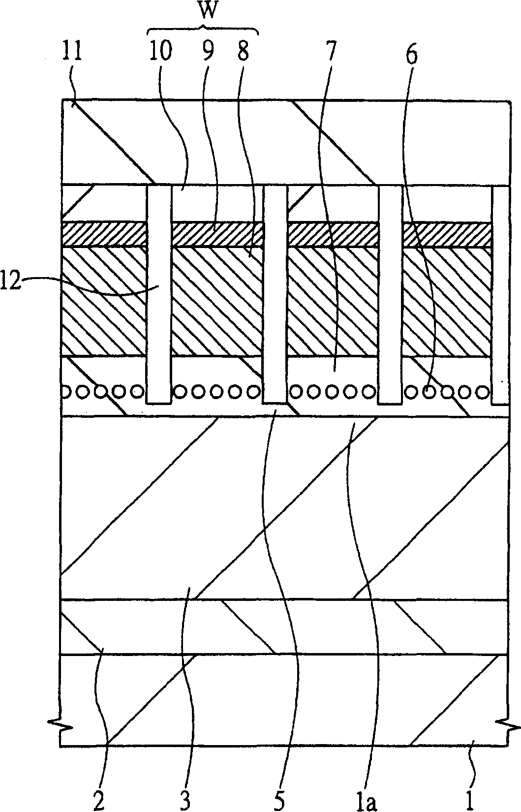
[0051] figure 1 is a schematic plan view showing a main part of a semiconductor substrate serving as a memory cell array of a flash memory according to this embodiment, figure 2 is along figure 1 The cross-sectional view of the semiconductor substrate of the A-B line (the cross-sectional direction of the auxiliary electrode), image 3 is along figure 1 The cross-sectional view of the semiconductor substrate of the C-D line (the cross-sectional direction of the word line), Figure 4 is an equivalent circuit diagram of the memory cell array. also, Figure 5 is the edge indicating the impurity concentration in each region of the memory cell ar...


PUM


Abstract

A nonvolatile semiconductor memory device that uses inversion layers formed on a surface of its semiconductor substrate as data lines, which is capable of satisfying the requirements of suppressing both characteristic variation among memory cells and bit cost. In order to achieve the above object, in the memory device, a plurality of assist gates are formed so as to be embedded in a p-type well via a silicon oxide film, respectively and silicon nanocrystal grains of about 6 nm in average diameter used for storing information are formed without being in contact with one another. Then, a plurality of word lines are formed practically in a direction vertically to the assist gates and the space between adjacent those of the plurality of word lines is set under 1 / 2 of the width (gate length) of the word lines. Consequently, the inversion layers formed at side faces of the assist gates will be used as local data lines, thereby the resistance is lowered and the writing characteristic variation among memory cells in a memory mat is suppressed.

Description

technical field [0001] The present invention relates to a semiconductor memory device and a method of manufacturing the same, and particularly relates to a technique effective when applied to a nonvolatile semiconductor memory device using an inversion layer formed on a semiconductor substrate as a data line. Background technique [0002] As an application for data storage with excellent portability, flash memory which is a semiconductor nonvolatile memory has begun to be widely used. The price per bit of the above-mentioned flash memory has been decreasing rapidly year by year, and the rate of decrease is faster than expected only from miniaturization. [0003] Among the memory cell array systems of large-capacity flash memory for file use, there are NAND type in which memory cells are connected in series and AND type in which memory cells are connected in parallel as typical systems. The former NAND type is described, for example, in F.Arai et al, IEEEInternational Electr...

Claims


Application Information

Patent Timeline
Patent Type & Authority Applications(China)
IPC IPC(8): G11C11/34G11C16/04H01L21/8239H01L21/8246H01L21/8247H01L27/10H01L27/115H01L29/788H01L29/792
CPCB82Y10/00G11C16/0475G11C16/0491H01L27/11521H01L27/115H01L27/11568H10B69/00H10B41/30H10B43/30
Inventor 石井智之峰利之笹子佳孝长部太郎
Owner RENESAS TECH CORP
Why Eureka
Try Eureka