Member for semiconductor device

A semiconductor and device technology, applied in the field of semiconductor devices, can solve the problems of low resin bonding strength, inability to achieve resin bonding strength, insufficient bonding strength, etc.

Inactive Publication Date: 2005-08-31
SUMITOMO ELECTRIC IND LTD
View PDF0 Cites 2 Cited by
  • Summary
  • Abstract
  • Description
  • Claims
  • Application Information

AI Technical Summary

Problems solved by technology

However, in Al and Cu, the bonding strength between the natural oxide film and the resin is insufficient, especially after the above-mentioned various reliability tests
In addition, alloys or composites mainly composed of Cu and W and / or Mo by themselves, such as Cu-W and Cu-Mo, cannot achieve satisfactory resin bond strength
This is because the natural oxide film of Cu is formed on some regions of alloys or composites mainly composed of Cu and W and / or Mo, but the resin bonding strength of these regions is low

Method used


Image

  • Member for semiconductor device
  • Member for semiconductor device
  • Member for semiconductor device

Examples


Embodiment Construction

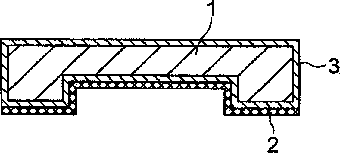
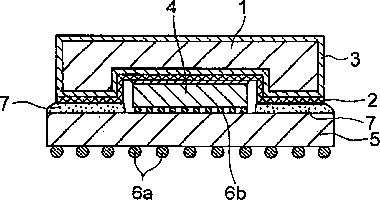
[0026] According to the present invention, the basic parts of parts used in semiconductor devices are made of alloys or composites mainly containing Cu and W and / or Mo, alloys or composites mainly containing Al-SiC, and alloys or composites mainly containing Si-SiC become. These alloys or composites have thermal expansion coefficients close to those of semiconductor components and packaging materials, and have excellent thermal conductivity. According to the present invention, when a part for a semiconductor device including a basic part made of these alloys or composites is bonded with other parts, such as a package, with resin, at least one surface of said basic part to be bonded by resin is provided A coating made of a thin film of solid carbon particles so that the bond strength of the resin can be increased.

[0027] The solid carbon particle film is amorphous carbon called diamond-like carbon, amorphous carbon, i-C or DLC (diamond carbon). Films of solid carbon particl...


PUM

PropertyMeasurementUnit
coating thicknessaaaaaaaaaa
diameteraaaaaaaaaa
thicknessaaaaaaaaaa

Abstract

There is provided a member for a semiconductor device, such as a substrate, having an excellent resin bonding property capable of improving resin bonding strength at the time the member for a semiconductor device being bonded with resin and maintaining a high resin bonding strength even after various reliability tests, such as a thermal cycling test, are performed. The member for a semiconductor device comprises a base member 1 made of an alloy or composite mainly composed of Cu and W and / or Mo, an alloy or composite mainly composed of Al-SiC, or an alloy or composite mainly composed of Si-SiC. A coating layer made of a hard carbon film 2 is provided on at least a surface of the base member 1 on which at least another member for the semiconductor device, such as a package, is bonded with a resin. It is preferable that the base member 1 have a surface roughness of 0.1 to 20 mu m in Rmax. It is preferable that the hard carbon film 2 have a thickness of 0.1 to 10 mu m.

Description

technical field [0001] Field of the Invention The present invention relates to components used in heat sinks, heat dissipation substrates, housings, etc. constituting semiconductor devices, and more particularly, to a semiconductor device having excellent resin bonding properties, and a semiconductor device utilizing such properties. Background technique [0002] When a substrate material constituting a part of a semiconductor device is bonded to a part used in another device, since thermal stress does not occur in the interface between the bonded parts, deformation is required. For this reason, the coefficient of thermal expansion of the substrate material must not be significantly different from that of other components of the semiconductor device, such as various semiconductor components or packages. Especially as the current semiconductor devices are made small and light, it is necessary to use materials with high thermal conductivity, and the thermal expansion coefficie...

Claims


Application Information

Patent Timeline
Patent Type & Authority Applications(China)
IPC IPC(8): H01L23/02H01L23/04H01L23/06H01L23/373
CPCH01L2224/73253H01L23/04H01L2924/01019H01L2924/15311H01L2924/01078H01L2924/16152H01L2924/01079H01L2224/16225H01L23/3732H01L23/06H01L2224/16H01L23/373H01L23/36
Inventor 上武和弥安部诱岳桧垣贤次郎
Owner SUMITOMO ELECTRIC IND LTD
Why Eureka
Try Eureka