
Soldering tin forming device, method and continuous plating device

A soldering and area technology, which is applied in the field of soldering area forming devices, can solve problems such as the fracture of the electroplating layer, and achieve the effect of improving mechanical strength and improving joint reliability.

Inactive Publication Date: 2005-09-21
MURATA KK
View PDF0 Cites 5 Cited by
  • Summary
  • Abstract
  • Description
  • Claims
  • Application Information

AI Technical Summary

Problems solved by technology

This leads to the following problems: the cracking of the plating layer due to the processing, or the deterioration of the wettability due to the deterioration of the corrosion resistance caused by the reduction of the plating base film such as nickel (nickel) to improve the workability, or the selection of materials is limited.

Method used


Image

  • Soldering tin forming device, method and continuous plating device
  • Soldering tin forming device, method and continuous plating device
  • Soldering tin forming device, method and continuous plating device

Examples


Embodiment approach 1

[0053] Regarding the first implementation mode, use Figure 1 to Figure 7 Be explained.

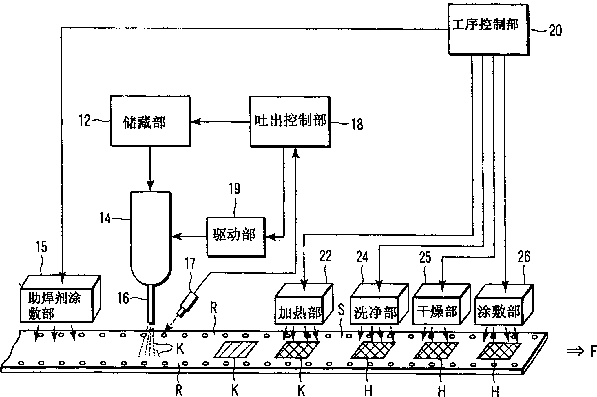
[0054] figure 1 It is a structural conceptual diagram showing an example of a solder forming apparatus to which the solder region forming method of the first embodiment is applied.

[0055] That is, the solder region forming apparatus is an apparatus for forming a solder region H on components S such as film carrier tapes, connector components, and lead frames, and includes a storage unit 12, a dispenser 14 provided with a nozzle 16 at the tip, and a flux Coating unit 15, position sensor (sensor) 17, discharge control unit 18, drive unit 19, process control unit 20, heating unit 22, cleaning unit 24, drying unit 25, coating unit 26, and conveyance unit (not shown) .

[0056] Process control unit 20 controls flux application unit 15 , heating unit 22 , cleaning unit 24 , drying unit 25 , and application unit 26 .

[0057] The flux application unit 15 applies a flux that promotes solder...

Embodiment approach 2

[0094] Referring to Figure 8, Figure 9 Embodiment 2 will be described. Embodiment 2 is a modified example of Embodiment 1. Therefore, only the differences are described here, and repeated descriptions are avoided.

[0095] FIG. 8 is a conceptual diagram showing the configuration of an example of a solder region forming apparatus to which the method of forming a solder region according to Embodiment 2 is applied.

[0096] That is, this solder region forming apparatus differs from Embodiment 1 only in that a plurality of distributors 14 and nozzles 16 are provided. The plurality of dispensers 14 and nozzles 16 also supply the solder paste K from the storage unit 12 . In addition, FIG. 8 shows the structure in this case: the solder paste K is supplied from the same storage part 12 to a plurality of distributors 14, but as Figure 9 As shown, a storage portion 12 corresponding to each dispenser 14 may also be provided.

[0097] In addition, Figure 8 and Figure 9 In the fig...


PUM


Abstract

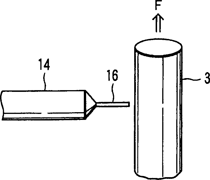
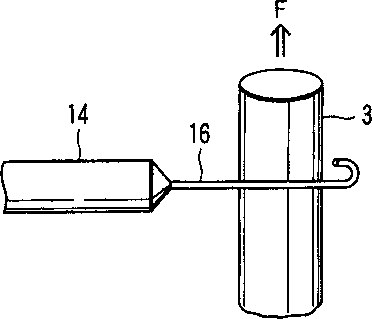
PROBLEM TO BE SOLVED: To form a solder region by solder paste, and to improve the reliability in joining, and the mechanical strength and quality of the solder itself.SOLUTION: The solder region formation device where a solder region H is formed on a member S is provided with: a storage part 12 of storing solder paste K; a dispenser 14 provided with a nozzle 16 discharging the solder paste K stored in the storage part 12 toward the member S; a discharge control part 18 of controlling the discharge amount and discharge rate of the solder paste K discharged from the nozzle 16; and a heating part 22 forming the solder region H on the member S by heating and melting the solder paste K discharged from the nozzle 16 in the dispenser 14 controlled by the discharge control part 18 and applied to the prescribed position.

Description

[0001] technology area [0002] The present invention relates to solder area forming device, method and continuous plating device, more specifically, relates to such as film carrier tape (film carrier tape), connector (connector) components and lead frame (lead frame), etc., by electronic components A device and method for forming solder regions on manufactured electronic components, and a continuous plating device for continuously forming solder regions on the aforementioned electronic components. Background technique [0003] The plating treatment of electronic components made of electronic components such as film carrier tapes, connector components, and lead frames is carried out as follows: the material wound into a coil (coil) is continuously fed into the wet plating device, and Roll up continuously after processing. This treatment is carried out by a continuous plating unit. As a representative example of such a continuous plating process, a connector part will be desc...

Claims


Application Information

Patent Timeline
Patent Type & Authority Applications(China)
IPC IPC(8): B23K3/06B23K1/20B23K101/36C23C24/08H01L21/60H01L23/50
CPCH01L24/743A41D13/0125A41D2600/20B63C9/11
Inventor 加藤和彦柳田贤佐藤修近藤峯雄
Owner MURATA KK
Learn More