Method of manufacturing tape wiring substrate

A substrate and circuit technology, applied in manufacturing tools, printed circuit manufacturing, multilayer circuit manufacturing, etc., can solve problems such as difficult circuit patterns, increased batches, and increased production costs

Inactive Publication Date: 2005-09-21
SAMSUNG ELECTRONICS CO LTD
View PDF1 Cites 19 Cited by
  • Summary
  • Abstract
  • Description
  • Claims
  • Application Information

AI Technical Summary

Problems solved by technology

[0010] Such many process steps cause an increase in the batch size of the production line and an increase in the batch size of materials consumed periodically, such as PR, PR developer, copper film etchant, etc., thus significantly increasing the production cost
[0011] In addition, since a light source 132 having a relatively large wavelength of several hundreds of micrometers is used in conventional photolithography and etching processes, it is difficult to form micrometer-order line patterns with a fine pitch on the copper film 120.

Method used


Image

  • Method of manufacturing tape wiring substrate
  • Method of manufacturing tape wiring substrate
  • Method of manufacturing tape wiring substrate

Examples


Embodiment Construction

[0023] Advantages and features of the present invention and methods of attaining the present invention will be more apparent and comprehensible by referring to the following detailed description of the preferred embodiments and accompanying drawings. This invention may, however, be embodied in many different forms and should not be construed as limited to the embodiments set forth herein. Rather, these embodiments are provided so that this disclosure will be thorough and complete and will fully convey the concept of the invention to those skilled in the art. Rather, the invention should only be defined by the appended claims. In the specification, similar symbols indicate similar components.

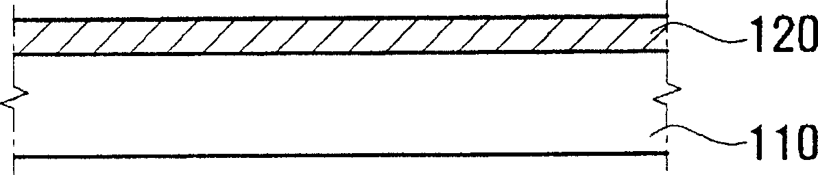
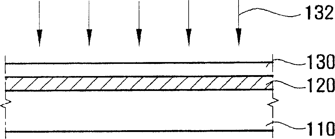
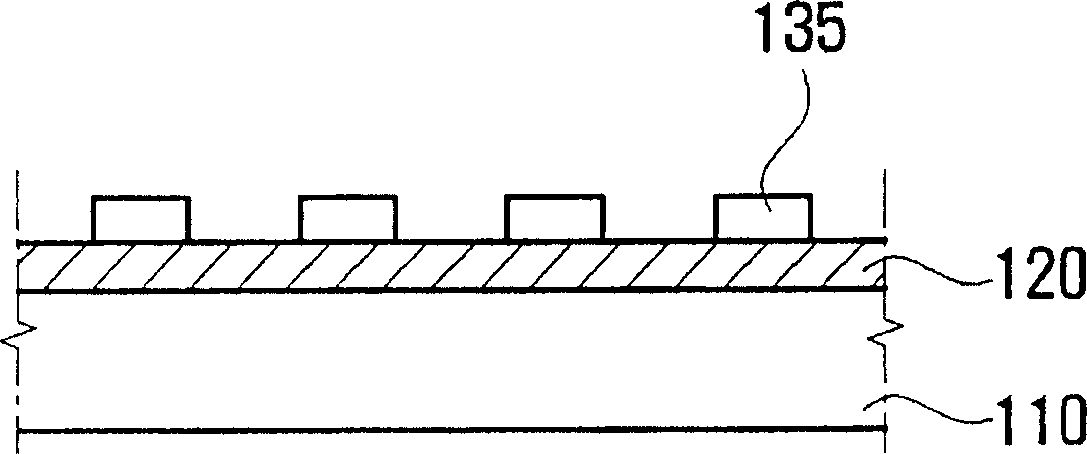
[0024] In one embodiment of the present invention, a flexible printed circuit board (FPC), such as a tape carrier package (TCP) or a chip on film (COF), may be used as a tape wiring substrate in which a wiring pattern is formed on a base film. A tape wiring substrate used in an embodim...


PUM

PropertyMeasurementUnit
thicknessaaaaaaaaaa
thicknessaaaaaaaaaa
thicknessaaaaaaaaaa

Abstract

A method of manufacturing a tape wiring substrate, by which the production cost can be reduced by a simplified manufacturing process. A fine wiring pattern having fine pitches can be formed. The method of manufacturing a tape wiring substrate includes preparing a base film, forming a metal layer on the base film, and processing the metal layer into a wiring pattern using a laser. In addition, the metal layer is partially removed using the laser, and a wiring pattern is formed by a subsequent wet etching.

Description

[0001] This application claims priority from Korean Patent Application No. 10-2004-0017943 filed on March 17, 2004 in the Korean Intellectual Property Office, the disclosure of which is incorporated by reference in its entirety. technical field [0002] The present invention relates to a method of manufacturing a tape wiring substrate, and more particularly to a method of manufacturing a tape wiring substrate using a laser to form a wiring pattern. Background technique [0003] Due to recent trends in thinness, compactness, high integration, high speed, and multiple leads of semiconductor devices, tape wiring substrates have been increasingly used in semiconductor chip mounting techniques. The tape wiring substrate is designed so that a wiring pattern layer is formed on a base film made of insulating material such as polyimide resin. Using tape automated bonding (TAB) technology, in a tape wiring substrate, wires connected to a wiring pattern layer can be bonded at one time ...

Claims


Application Information

Patent Timeline
Patent Type & Authority Applications(China)
IPC IPC(8): B23K26/36B23K101/42C23F1/00C23F1/18C23F4/00C23F4/02H01L21/60H05K3/00H05K3/02H05K3/06H05K3/08H05K3/46
CPCH05K2203/1121H05K2203/1476C23F4/02H05K3/06H05K3/027C23F1/02H05K2203/0783H05K2203/0369C23F1/18H01L21/60
Inventor 李忠善姜思尹权容焕崔敬世
Owner SAMSUNG ELECTRONICS CO LTD
Why Eureka
Try Eureka