Method for making self-alignment type thin-film transistor

A technology for thin film transistors and manufacturing methods, which is applied in the manufacture of transistors, semiconductor/solid-state devices, electrical components, etc., can solve the problem of uneven chromaticity, and achieve the effect of solving uneven chromaticity and simplifying the TFT process.

Inactive Publication Date: 2005-10-05
AU OPTRONICS CORP
View PDF1 Cites 16 Cited by
  • Summary
  • Abstract
  • Description
  • Claims
  • Application Information

AI Technical Summary

Problems solved by technology

[0009] According to the present invention, since the transparent conductive material is used as the material of the drain electrode and the source electrode in the utilization of step (ii), and its light-transmitting characteristics are utilized, when using a negative photoresist (the exposed part remains, the unexposed part The part can be etched and removed) and use the first metal layer (gate) as a photomask to perform back exposure, and then perform etching to etch and remove the part corresponding to the gate metal, so as to reach the drain, source and gate The purpose of precise alignment, and then solve the problem of uneven chromaticity caused by uneven gate-to-drain capacitance (Cgd) in the traditional yellow light process

Method used


Image

  • Method for making self-alignment type thin-film transistor
  • Method for making self-alignment type thin-film transistor
  • Method for making self-alignment type thin-film transistor

Examples


Embodiment Construction

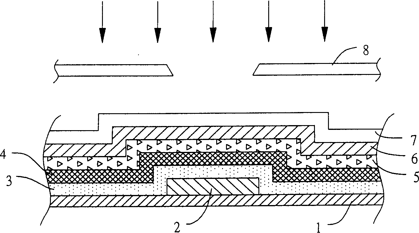
[0018] In the description of the present invention, the term "backside exposure" or "exposure from the substrate side" refers to illuminating light toward the substrate from the side of the substrate on which no pattern or material layer is formed.

[0019] On the contrary, the term "front exposure" or "exposure from the opposite side of the substrate" in the present invention means that light is illuminated toward the substrate from the side of the substrate on which the pattern or material layer is formed.

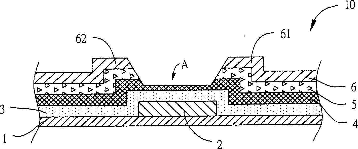
[0020] The manufacturing method of the self-aligned thin film transistor of the present invention will be described in more detail with reference to the following drawings.

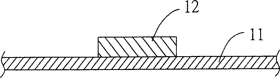
[0021] Please refer to FIG. 2 , in which a metal layer 12 with a desired pattern is formed on a substrate 11 by photolithographic etching as a gate. The substrate 11 used therein is a transparent material such as glass, quartz or plastic. The gate 12 can be any conductive metal used in the TFT fiel...


PUM


Abstract

The method includes following steps: plating a layer of metal on a base plate; forming needed pattern of gate by using mask preparation procedure; developing gate insulation layer, semiconductor layer, ohmic contact layer and transparent conducting layer in sequence; carrying out exposure in backside by using negative photoresistive agent and gate metal as mask; carrying out etching and general multiple layers semiconductor fabricating procedures so as to obtain source pole and drain pole aligned to gate pole. The invention improves issue of uneven chromaticity (mura) of LCD caused by drain capacitance of gate (Cgd).

Description

technical field [0001] The invention relates to a manufacturing method of a drain, source and gate self-aligned thin film transistor. [0002] In particular, the present invention relates to a manufacturing method of a self-aligned drain, source, and gate TFT by using transparent electrodes and exposing from the substrate side (back surface) to improve the chromaticity unevenness (mura) of a liquid crystal display. Background technique [0003] The existing thin-film transistor (TFT) preparation method in liquid crystal displays, as shown in Figure 1a, generally coats a metal electrode 2 with a desired pattern on a substrate 1 as a gate, and then grows a gate insulating layer 3. , grow an amorphous silicon layer 4, an n+ silicon layer 5 and a metal layer 6 in sequence, and then coat a layer of positive photoresist layer 7 on the metal layer, expose through a photomask 8 with a desired pattern, and then The positive photoresist layer 7 is etched away in the exposed area, and...

Claims


Application Information

Patent Timeline
Patent Type & Authority Applications(China)
IPC IPC(8): H01L21/336H01L29/786
Inventor 黄茂村
Owner AU OPTRONICS CORP
Why Eureka
Try Eureka