Thin film capacitor and method for manufacturing same
A technology of film capacitors and electrodes, applied in the field of capacitors, can solve the problems of sharp reduction and no performance
- Summary
- Abstract
- Description
- Claims
- Application Information
AI Technical Summary
Problems solved by technology
Method used
Image
Examples
Embodiment Construction
[0039] The inventors of the present invention discovered that a single crystal lower electrode and a single crystal dielectric layer can be grown on a single crystal silicon substrate.
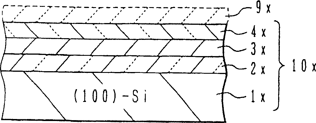
[0040] Figure 1A represents the structure of the sample. A silicon substrate 1x having a (100) plane is prepared. Using SrTiO 3 Sputtering target, containing Ar and O 2 Ar / O 2 At a substrate temperature of 800°C, RF sputtering was used to form SrTiO with a thickness of about 100 nm on the (100) surface of the silicon substrate. 3 The film 2x serves as an intermediate layer of insulating material.
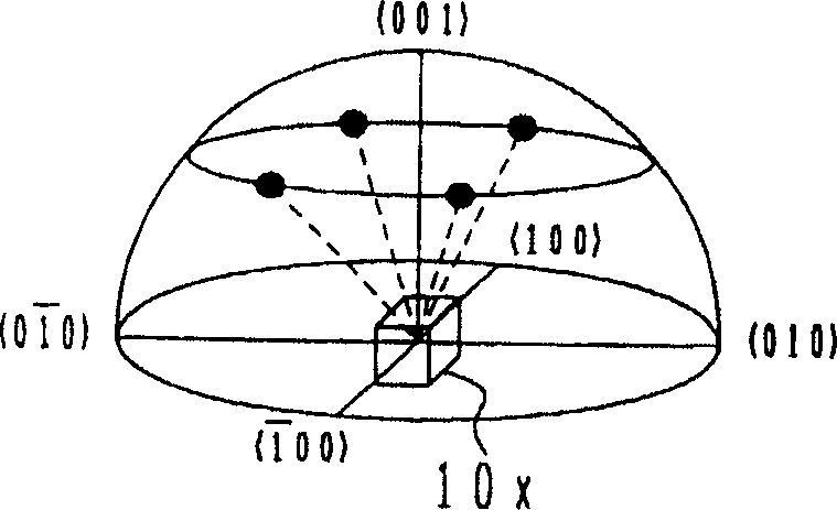
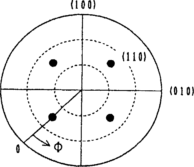
[0041] The substrate temperature was set to 600° C., a Pt layer 3x with a thickness of about 500 nm was formed as a lower electrode layer on the intermediate layer 2x by DC sputtering in an Ar atmosphere, and Ar / O was passed thereon. 2Atmospheric RF sputtering forms ~50 nm thick BaSrTiO of high dielectric constant perovskite oxides 3 Layer 4x acts as a dielectric layer. The sample 10x was p...
PUM
| Property | Measurement | Unit |
|---|---|---|
| coating thickness | aaaaa | aaaaa |
| coating thickness | aaaaa | aaaaa |
| coating thickness | aaaaa | aaaaa |
Abstract
Description
Claims
Application Information


