
Standard unit overall wiring method of multi-terminal network plug-in buffer optimizing delay

A technology of overall wiring and standard cells, applied in instruments, special data processing applications, electrical digital data processing, etc., can solve the problem that the algorithm cannot be directly applied to the multi-terminal wire network.

Inactive Publication Date: 2005-10-26
TSINGHUA UNIV
View PDF1 Cites 13 Cited by
  • Summary
  • Abstract
  • Description
  • Claims
  • Application Information

AI Technical Summary

Problems solved by technology

However, in the actual layout process, the algorithm for two-terminal nets often cannot be directly applied to multi-terminal nets, so the buffer insertion algorithm for two-terminal nets has certain limitations

Method used


Image

  • Standard unit overall wiring method of multi-terminal network plug-in buffer optimizing delay
  • Standard unit overall wiring method of multi-terminal network plug-in buffer optimizing delay
  • Standard unit overall wiring method of multi-terminal network plug-in buffer optimizing delay

Examples


Embodiment Construction

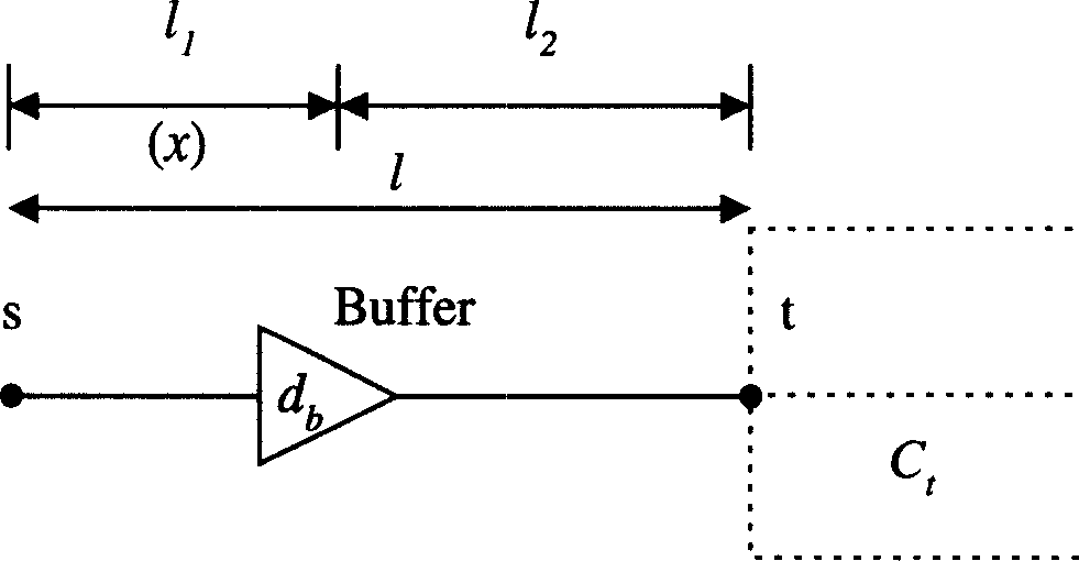
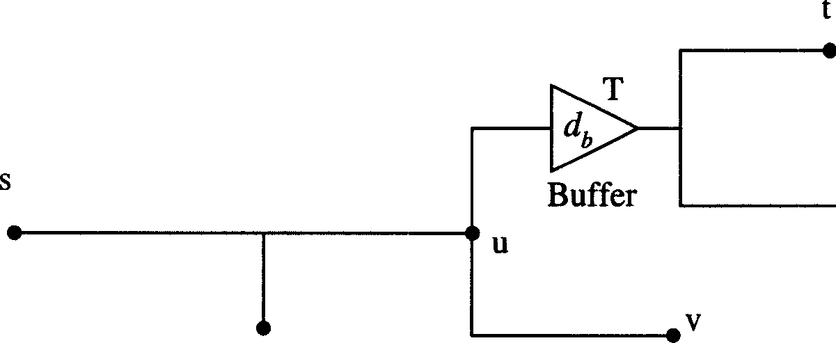
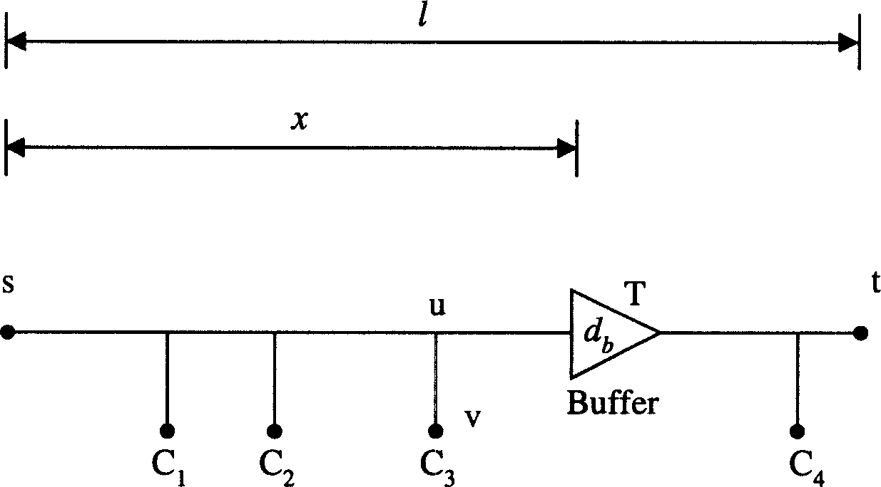
[0106] First, the optimal position for inserting a single buffer in the multi-terminal net to obtain the maximum delay improvement is deduced, and the formula for solving the optimal position is obtained. The derivation process includes two steps. The first step is to deduce the optimal position where the two-point line net is inserted into the buffer. In the second step, the optimal position for inserting the buffer of the multi-terminal net is derived.

[0107] The derivation process is based on the well-known "SAKURAI delay calculation formula", and a brief introduction to the "SAKURAI delay calculation formula" is given below.

[0108] The calculation formula of SAKURAI time delay regards the interconnection line as a transmission line with distributed resistance and capacitance, and the calculation formula is basically the same as the actual situation. The delay calculation formula is:

[0109] T DZ =βR s (c e +C z )+αr e c e +βr e C z

...


PUM


Abstract

The invention is a standard cell general wiring method for optimizing time delay by inserting buffers in multi-end line network, belonging to IC CAD technical field, and characterized in: as optimizing circuit time delay, firstly using the known standard cell general wiring method that optimizes the time delay based on key network technique to construct a key network for the circuit, and then using the minimum cutting method to find a group of line networks obviously optimizing time delay but little worsening the jam; after replacing a multi-end line network among them with a time delay optimum wiring tree, in the paths from source node to key drain points, firstly converting the time delay optimum wiring tree to a branched wiring tree, then according to the SAKURAI time delay calculating formula, selecting a node with the maximum improved value from the optimum insert point and branched insert point in the path during time delay improving; then judging if the node accords to initial restriction index. Relative to the traditional methods, the invention can obtain the outstanding time delay optimized result within a shorter time.

Description

technical field [0001] Integrated circuit computer aided design is the technical field of IC CAD, especially related to the field of standard cell (SC) overall wiring design. Background technique [0002] In integrated circuit (IC) design, physical design is the main link in the IC design process, and it is also the most time-consuming step. A computer-aided design technique related to physical design is called layout design. In layout design, overall wiring is an extremely important link, and its results have a great influence on the success of the final detailed wiring and the performance of the chip. [0003] In the deep submicron (Deep Submicron, DSM) and very deep submicron (VDSM) process stages of integrated circuits, interconnection delay becomes a decisive factor affecting circuit performance. To optimize the performance of the chip, performance optimization goals such as latency must be considered. In circuit delay optimization, buffer insertion technique is a ve...

Claims


Application Information

Patent Timeline
IPC IPC(8): G06F17/50
Inventor 洪先龙经彤许静宇
Owner TSINGHUA UNIV
Learn More