

Lomposite metallic inorganic source of zirconium hafnium and titanium composited anhydrous nitrate and its synthesis method
A technology of metal compounding and synthesis methods, applied in inorganic chemistry, titanium compounds, zirconium compounds, etc., can solve the problems of large differences in thermal evaporation and thermal decomposition properties of organic compounds, deterioration of film properties, low dielectric constant, etc. Low, good volatility, low deposition temperature effect
- Summary
- Abstract
- Description
- Claims
- Application Information
AI Technical Summary
Problems solved by technology
Method used
Image

Examples
Embodiment Construction
[0011] Synthetic raw material: fuming nitric acid (HNO 3 ), phosphorus pentoxide (P 2 o 5 ), titanium tetrachloride (TiCl 4 ), anhydrous zirconium tetrachloride (ZrCl 4 ), hafnium tetrachloride (HfCl 4 ). ZrCl can be controlled arbitrarily 4 , HfCl 4 with TiCl 4 Generally speaking, the ratio of raw materials is selected in the range of 0.9≥x≥0.1, 0.9≥y≥0.1.
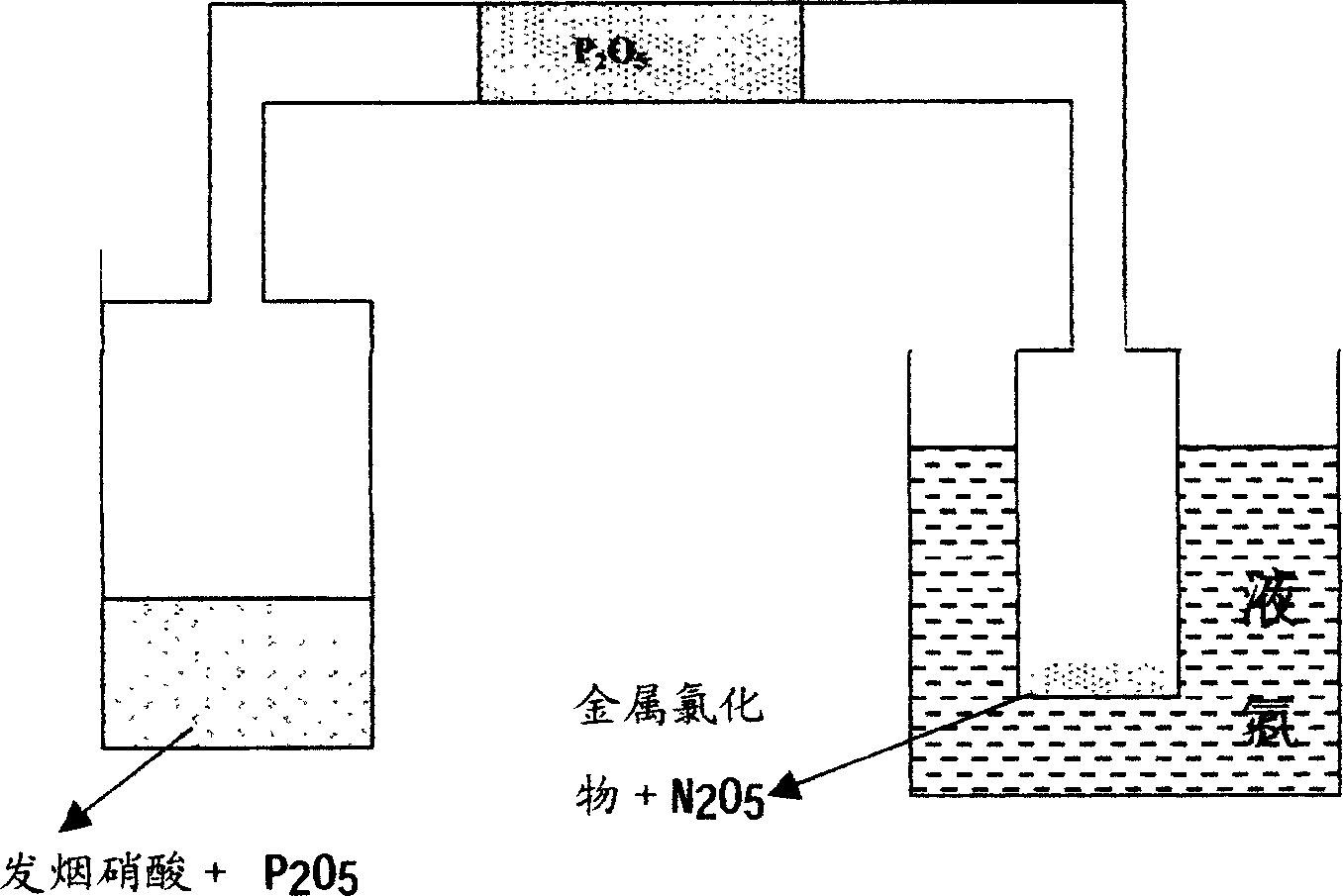
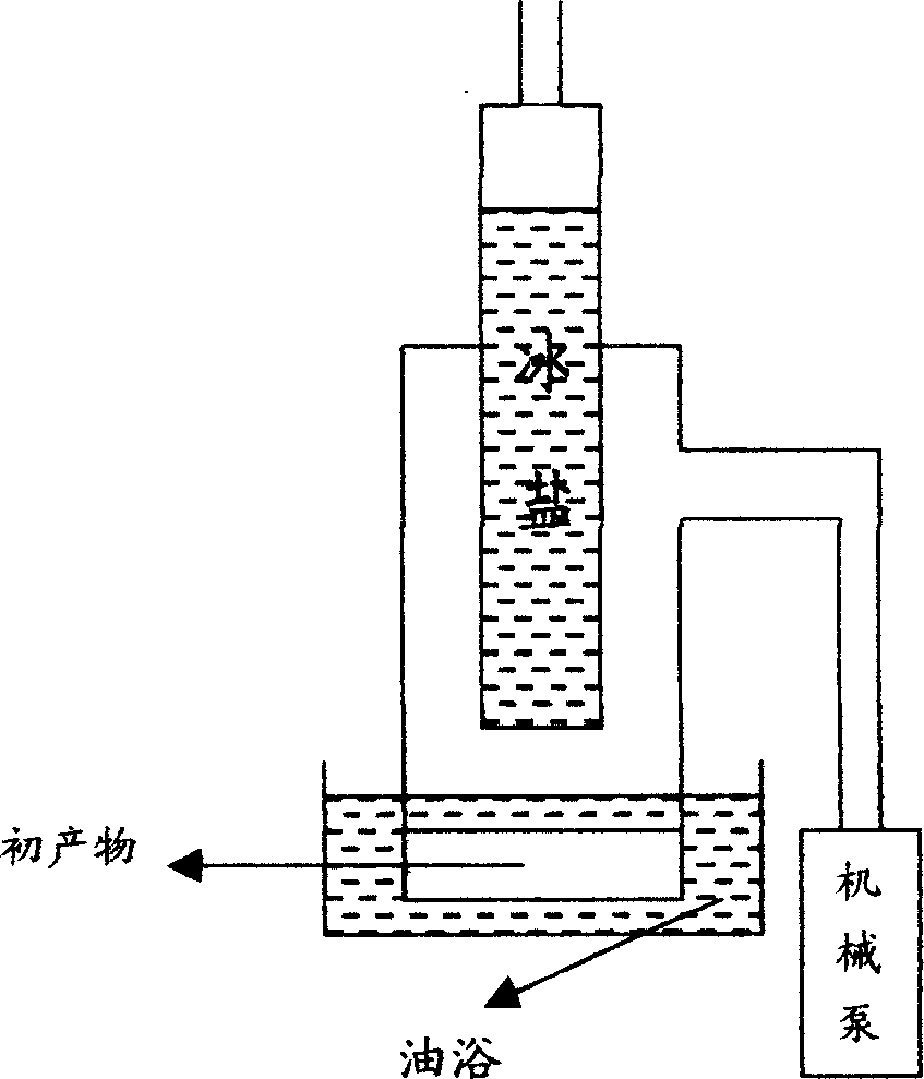
[0012] Volatile zirconium titanium anhydrous nitrate (Zr 1-x Ti x )(NO 3 ) 4 The synthesis process: the schematic diagram of the synthesis device is as follows Figure 1 As shown, all the connections are made of ground joints, which are communicated with the atmosphere through the phosphorus pentoxide drying tube to prevent the moisture in the environment from entering the system. Anhydrous nitrate is prepared from liquid dinitrogen tetroxide (N 2 o 4 ) with different proportions of TiCl 4 and ZrCl 4 It reacts at room temperature. TiCl 4 and ZrCl 4 Pre-placed in a glass reactor, the glass reactor was i...
PUM
 Abstract
Description
Claims
Application Information