Mutual compensating metals-oxides-semiconductor structure and its mfg. method

A complementary metal and semiconductor technology, applied in semiconductor/solid-state device manufacturing, semiconductor devices, transistors, etc., can solve problems such as threshold voltage and flat-band voltage change

Inactive Publication Date: 2005-11-16
INT BUSINESS MASCH CORP
View PDF3 Cites 11 Cited by
  • Summary
  • Abstract
  • Description
  • Claims
  • Application Information

AI Technical Summary

Problems solved by technology

[0008] The present invention adds an insulating interlayer between the high κ gate dielectric layer and the Si-containing gate conductor, which solves the above-mentioned problem of threshold voltage and flat-band voltage change

Method used


Image

  • Mutual compensating metals-oxides-semiconductor structure and its mfg. method
  • Mutual compensating metals-oxides-semiconductor structure and its mfg. method
  • Mutual compensating metals-oxides-semiconductor structure and its mfg. method

Examples


example 1

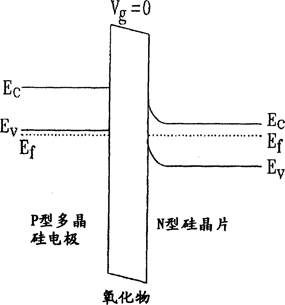
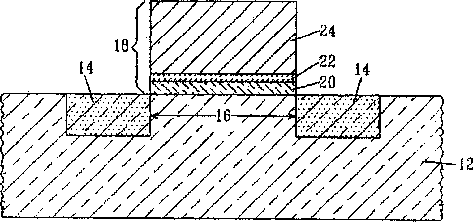
[0062] In this example, a Hf oxide or silicate layer is first grown on a silicon wafer prefabricated with a field oxide pattern. The Hf oxides and silicates are deposited by metalorganic chemical vapor deposition (MOCVD) and atomic layer chemical vapor deposition (ALCVD). The thickness of Hf oxide and silicate layer is about 2-4nm, and the composition of silicate is close to Hf x Si y o 4 , where y / (x+y) is about 0.2-0.3. These oxides are deposited on n-type silicon wafers covered with silicon oxide or silicon oxynitride with a thickness of 0.3-1.2 nm. The presence of this layer is completely optional.

[0063] After depositing Hf oxide and silicate, the wafer is loaded into an ultra-high vacuum deposition chamber to deposit aluminum nitride. Aluminum nitride was deposited by evaporating Al from a resistively heated standard Al jet furnace and using a nitrogen beam from a commercial radio frequency atomic nitrogen source. The temperature of the spray furnace during depos...


PUM


Abstract

PROBLEM TO BE SOLVED: To provide a complementary metal-oxide semiconductor (CMOS) structure including an intermediate layer between a Si-containing gate electrode and a high-k gate dielectric, so that a threshold voltage and a flat-band voltage of the structure are stabilized.

Description

technical field [0001] The present invention relates generally to semiconductor devices, and more particularly to a complementary metal-oxide-semiconductor structure (CMOS) having an interlayer between its Si-containing gate electrode and a high-κ gate dielectric layer capable of The threshold voltage and flatband voltage of this structure are stabilized. Background technique [0002] In standard silicon complementary metal-oxide-semiconductor (CMOS) technology, a p-type field-effect transistor (pFET) uses a p-type polysilicon layer doped with boron (or other acceptor elements) as the gate electrode, which is deposited on a silicon dioxide or silicon oxynitride gate oxide. The gate voltage applied through this polysilicon layer creates an inversion channel in the n-type silicon under the gate oxide layer. [0003] For a pFET to work properly, inversion should begin when a slightly negative voltage is applied to the polysilicon (poly-Si) gate electrode. for figure 1 For t...

Claims


Application Information

Patent Timeline
Patent Type & Authority Applications(China)
IPC IPC(8): H01L21/8234H01L21/28H01L21/8238H01L27/088H01L27/092H01L29/49H01L29/51H01L29/76H01L29/78H01L29/786H01L51/00H01L51/05
CPCH01L29/518H01L21/28202H01L21/823857H01L29/4916H01L29/513H01L21/28194H01L29/517
Inventor 小内斯特·A.·伯加克祖克埃杜阿德·A.·卡特尔马丁·M.·弗兰克爱维格尼·果塞弗撒普拉迪克·古哈维嘉·纳拉亚纳恩
Owner INT BUSINESS MASCH CORP
Why Eureka
Try Eureka