Semiconductor device and method for manufacturing same
A semiconductor and device technology, applied in the field of semiconductor devices and their manufacturing, can solve the problems of increased dispersion of sheet resistance, increased junction leakage current, and large roughness
- Summary
- Abstract
- Description
- Claims
- Application Information
AI Technical Summary
Problems solved by technology
Method used
Image

Examples
no. 1 example
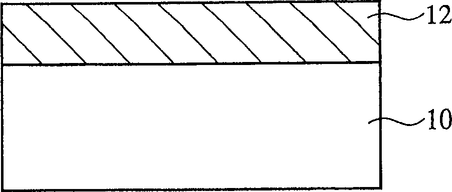
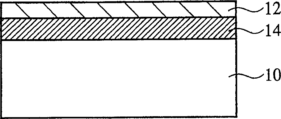
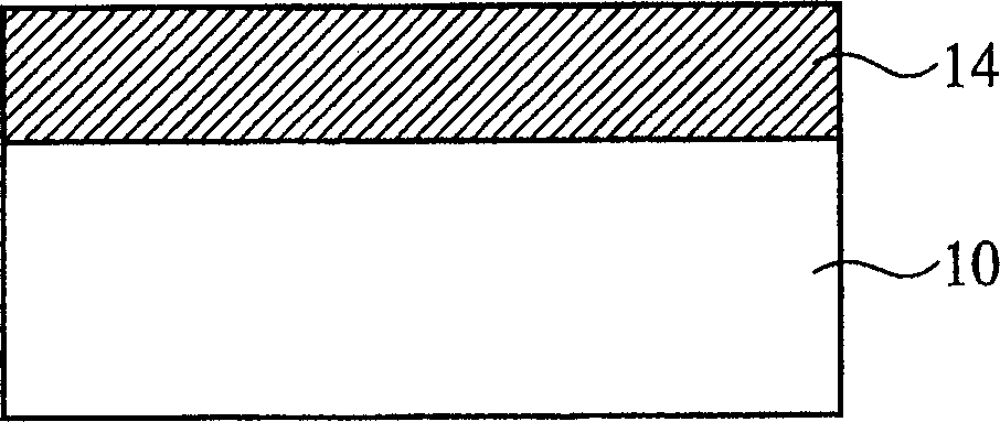
[0072] will refer to Figures 7 to 22 , a description will be given of a semiconductor device and a manufacturing method thereof according to a first embodiment of the present invention. Figure 7 is a sectional view of the semiconductor device according to the present embodiment. Figures 8A-8C 18A to 18C are cross-sectional views of the semiconductor device according to the present embodiment in steps of a method for manufacturing the semiconductor device, which illustrate the method. Figures 19A-19D is a transmission electron microscope picture showing the evaluation results of the method for manufacturing the semiconductor device according to this embodiment. Figure 20 is a cross-sectional view of a semiconductor device used in evaluating the method for manufacturing the semiconductor device according to the present embodiment, showing its structure. Figure 21 with 22 is a graph of the evaluation results of the method for manufacturing the semiconductor device accord...
no. 2 example
[0180] will refer to Figures 23A to 23C , explain a semiconductor device and a method for manufacturing the semiconductor device according to a second embodiment of the present invention. Figures 23A to 23C are cross-sectional views of the semiconductor device according to the present embodiment in the steps of a method for manufacturing the semiconductor device, which illustrate the method. This embodiment and according to Figures 7 to 18A The same elements of the semiconductor device and its manufacturing method of the first embodiment shown in -18C are denoted by the same reference numerals to avoid repetition or to simplify their description.
[0181] The semiconductor device according to the present embodiment is basically the same in structure as the semiconductor device according to the first embodiment, but differs from the latter in the method of manufacturing the semiconductor device.
[0182] That is, the method for manufacturing the semiconductor device accord...
PUM
| Property | Measurement | Unit |
|---|---|---|
| thickness | aaaaa | aaaaa |
| thickness | aaaaa | aaaaa |
| thickness | aaaaa | aaaaa |
Abstract
Description
Claims
Application Information
 - R&D
- Intellectual Property
- Life Sciences
- Materials
- Tech Scout
- Unparalleled Data Quality
- Higher Quality Content
- 60% Fewer Hallucinations
Browse by: Latest US Patents, China's latest patents, Technical Efficacy Thesaurus, Application Domain, Technology Topic, Popular Technical Reports.
© 2025 PatSnap. All rights reserved.Legal|Privacy policy|Modern Slavery Act Transparency Statement|Sitemap|About US| Contact US: help@patsnap.com