Method of enhancing clear field phase shift masks by adding parallel line to phase 0 region

A technology of area and phase, which is applied in the direction of circuit, electrical components, and patterned surface photolithography, can solve the problems of complex patterning of binary masks and limitations of manufacturing window technology, so as to reduce the influence of aberration and reduce the The effect of aberration

Inactive Publication Date: 2005-11-23
GLOBALFOUNDRIES U S INC MALTA
View PDF3 Cites 0 Cited by
  • Summary
  • Abstract
  • Description
  • Claims
  • Application Information

AI Technical Summary

Problems solved by technology

As such, the patterning of the binary mask can be compl

Method used


Image

  • Method of enhancing clear field phase shift masks by adding parallel line to phase 0 region
  • Method of enhancing clear field phase shift masks by adding parallel line to phase 0 region
  • Method of enhancing clear field phase shift masks by adding parallel line to phase 0 region

Examples


Embodiment Construction

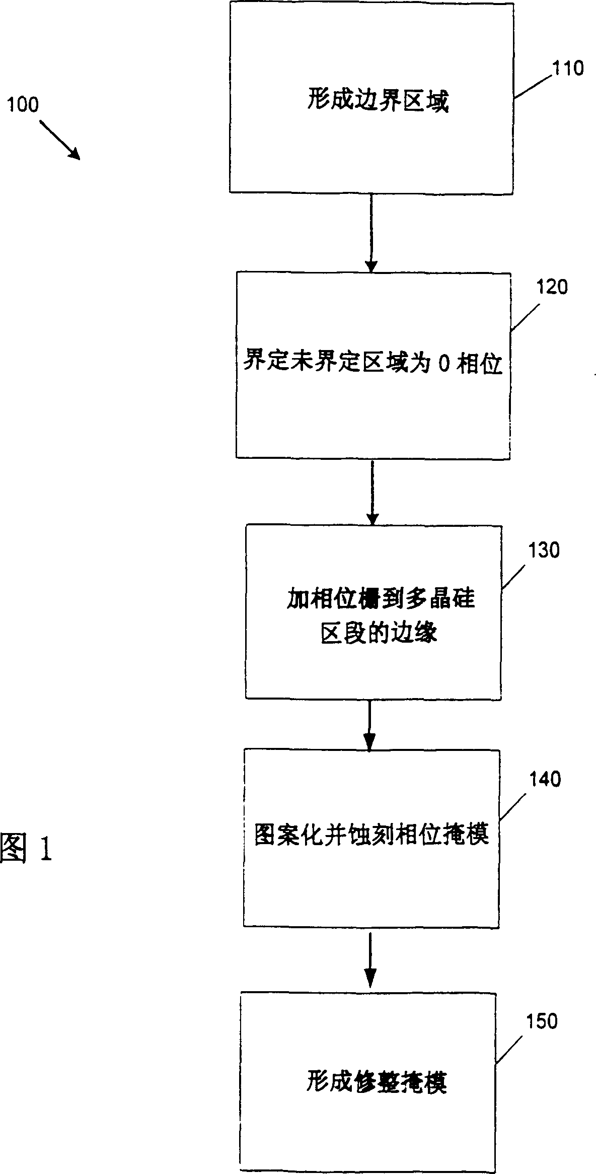
[0029] A flowchart 100 is shown in FIG. 1 to describe typical steps in the composition or design of a phase shift mask (PSM) and an electric field or trim mask. A set of pre-defined 0-phase or 180-phase boxes on the phase mask are used to identify a critical polysilicon region. The 0-phase or 180-phase cassettes can be generated by hand, using currently available software programs, or generating an optimal program to define the cassettes.

[0030] In step 110, a chromium border region is formed on the outside of the phase mask at the 180 phase cassette edge of the predefined 180 phase cassette that does not define a final polysilicon patterning. The chrome border area can be defined either by hand or using a computer software program. It is characterized in that the chromium border area allows easy inspection of the mask and easy patterning of the etch step that produces the mask. At step 120, all undefined areas (whether in the final pattern or 180 phase cassette or chrome ...


PUM


Abstract

A technique in which a boundary region is added to the outside parallel edge of phase zero (0) pattern defining polygons. This technique can reduce the need for optical proximity correction (OPC) and improve the manufacturability and patterning process window for integrated circuits. The technique can also set the width of both 0 and phase 180 polygons to specific sizes, making OPC easier to assign.

Description

technical field [0001] The present invention relates to integrated circuits and methods of fabrication thereof, and more particularly to generating phase shift patterns to improve patterning of gates, regions, structures, and layers requiring sub-nominal dimensions. Background technique [0002] A semiconductor device or an integrated circuit may contain a plurality of devices, such as transistors. Ultra-large ULSI may include complementary metal-oxide-semiconductor (CMOS) field-effect transistors (FETs). Although known systems and fabrication allow the fabrication of many IC devices on a single IC, there is still a need to reduce the size of the IC device body, thereby allowing an increase in the number of devices on a single IC. [0003] One limitation to achieving reduced IC device size is known lithography capabilities. Photolithography is the manufacturing process by which patterns or images are transferred from one medium to another. The known IC photolithography ut...

Claims


Application Information

Patent Timeline
IPC IPC(8): G03F1/00G03F1/30G03F7/20H01L21/027
CPCG03F1/144G03F1/30G03F1/70G03F1/36
Inventor T·P·卢康科C·A·斯彭斯
Owner GLOBALFOUNDRIES U S INC MALTA
Why Eureka
Try Eureka