Light wave guide device,light source device and light information processor

A technology of optical waveguide and multiplexing, applied in the direction of optical waveguide light guide, light guide, optics, etc., can solve the problems of increased loss and polarization dependence, and achieve the effect of small light loss and increased productivity

Inactive Publication Date: 2006-01-04
SONY CORP
View PDF1 Cites 3 Cited by
  • Summary
  • Abstract
  • Description
  • Claims
  • Application Information

AI Technical Summary

Problems solved by technology

In the case of light with unrestricted polarization such as LEDs, when it is desired to transmit light of one wavelength within a narrow wavelength range and reflect light of other wavelengths, if the incident light is placed at an angle as large as 45 degrees It is well known that the reflectance and transmittance of the filter are highly dependent on polarization and the loss becomes large when the incident light is incident on the filter.

Method used


Image

  • Light wave guide device,light source device and light information processor
  • Light wave guide device,light source device and light information processor
  • Light wave guide device,light source device and light information processor

Examples


Embodiment approach 1

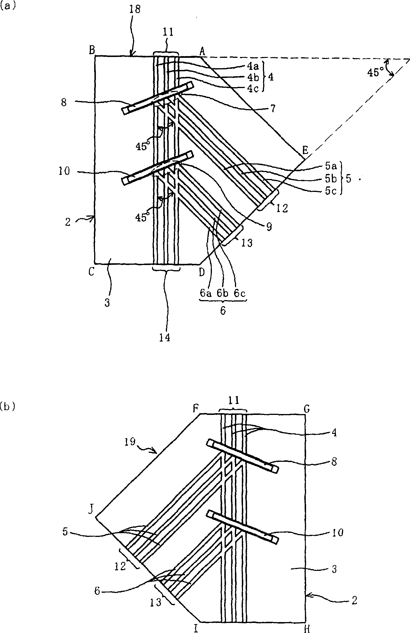
[0109] Embodiment 1 relates to an optical waveguide device having a pentagonal shape as an example of the optical waveguide device of the present invention, and a light source device using the optical waveguide device, and hereby uses Figure 1 to Figure 4 Be explained.

[0110] figure 1 (a) is a plan view of the optical waveguide device 18 according to the first embodiment. In this optical waveguide device 18, an optical waveguide layer 2 composed of a bonded body of a cladding layer 3 and core wires 4 to 6 is formed on a substrate 1 (not shown) such as silicon, and the lower cladding layer and the upper cladding layer A light guiding path, that is, a core wire, is embedded therebetween.

[0111] The optical waveguide layer 2 is made of, for example, an acrylic organic solvent, the refractive index of the cladding 3 is 1.505, the refractive index difference Δn between the core wires 4-6 and the cladding layer 3 is 0.8%, and the cross-section of the core wires 4-6 is 10 μm×...

Embodiment approach 2

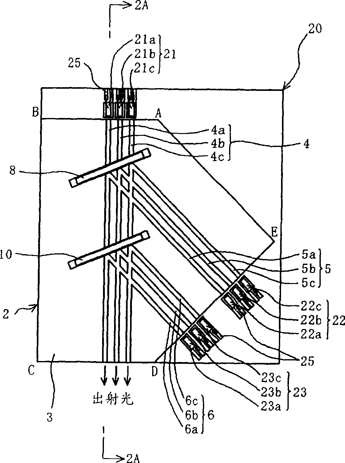
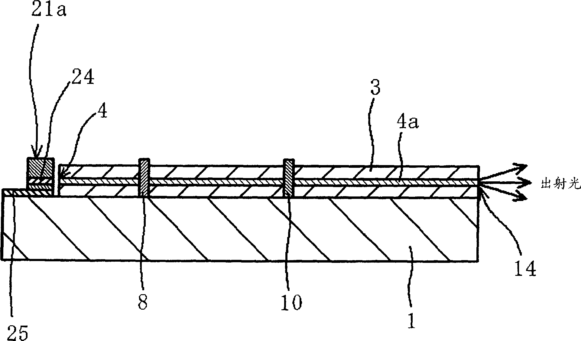
[0131] Embodiment 2 is an example of an optical waveguide device 28 , a light source device using the same, and an optical information processing device. This optical waveguide device 28 is obtained by modifying the optical waveguide device 18 based on Embodiment 1 as follows. The waveguide end faces of the side AB and side DE of the optical waveguide device 18 are subjected to 45-degree inclined processing, and the light incident end faces of the core wires 4 to 6 are formed into inclined reflective end faces, and the light is guided to the inside and outside of each core wire through these reflective end faces. .

[0132] By doing so, it is possible to use a surface-emitting light-emitting element and a surface-receiving light-receiving element. For example, surface-emitting LEDs are easy to manufacture, inexpensive, commercially available in many varieties, excellent in high-frequency characteristics, easy to modulate, and easy to install. In addition, light-receiving elem...

Embodiment approach 3

[0147] Embodiment 3 relates to an optical waveguide device having a square shape as an example of the optical waveguide device of the present invention, and a light source device using the optical waveguide device. Figure 8-10 Let me explain.

[0148] Figure 8 It is a plan view of the optical waveguide device 50 according to the third embodiment. In this optical waveguide device 50, an optical waveguide layer 52 composed of a bonded body of a clad 53 and core wires 54 to 56 is formed on a substrate 1 (not shown) such as silicon, and the lower clad and upper clad The waveguide core wire is buried between the cladding layers.

[0149] The optical waveguide layer 2 is the same as Embodiment 1. For example, it is made of an acrylic organic solvent. The refractive index of the cladding 53 is 1.505. The refractive index difference Δn between the core wires 54-56 and the cladding layer 53 is 0.8%. The cross section of 56 is a square of 10 μm×10 μm.

[0150] The cladding layer 5...


PUM


Abstract

To provide an optical waveguide device which is small in light loss , can be made small in size and low in cost, is small in the polarization dependency of transmittance and reflectance by a filter, and multiplexes or demultiplexes a plurality of light beams having different wavelength by segmenting the wavelength of transmitted light and the wavelength of reflected light in a narrower range, and to provide a light source device suitable as a point light source device for a compact display or the like and an optical information processing device which use the optical waveguide device. An optical waveguide layer 2 composed of an assembly of a clad 3 having the shape of a pentagon ABCDE where a side DE and a side BA cross at an acute angle of 45 degrees, and cores 4 to 6 is formed in the optical waveguide device. The core 4 is linearly provided from the side AB to a side CD nearly perpendicularly to the side AB, and the cores 5 and 6 are linearly provided from the side DE to a crossing part 7 or 9 crossing with the core 4 nearly perpendicularly to the side DE. Wavelength selecting filters 8 and 10 are provided at the crossing parts so as to part the core 4. In multiplexing the light, light is made incident from light incident or emitting end faces 11 to 13, and multiplexed light is taken out from a light emitting or incident end face 14.

Description

technical field [0001] The present invention relates to an optical waveguide device for multiplexing or splitting multiple beams of light having different wavelengths, a light source device using the same, suitable for use as a point light source device such as a small display, and an optical information processing device. Background technique [0002] In recent years, miniaturization, weight reduction, and multifunctionalization of electronic equipment, especially portable electronic equipment, etc. are being demanded. In this trend, image data is also being processed on portable electronic devices, and how to realize the function of displaying fine images easily has become a subject of research. [0003] For example, the retinal display disclosed in Japanese Patent Application Publication No. 11-505627, etc., can reduce the area occupied by the screen display because the image is formed on the retina of the user's eye, and can achieve both miniaturization and high-precisio...

Claims


Application Information

Patent Timeline
Patent Type & Authority Applications(China)
IPC IPC(8): G02B6/12G02B6/293H01L33/48
Inventor 成瀬晃和
Owner SONY CORP
Why Eureka
Try Eureka