
Emulating method and device for exposure system

A technology of an exposure system and a simulation method, which is applied to a photoplate-making process exposure device, a microlithography exposure device, and an input/output process of data processing, etc., can solve the problem of low accuracy of the simulation device and low accuracy of the simulation method of the exposure system. and other problems to achieve the effect of shortening the design cycle, speeding up the design progress and high accuracy

Inactive Publication Date: 2006-01-04
HONG FU JIN PRECISION IND (SHENZHEN) CO LTD +1
View PDF0 Cites 2 Cited by
  • Summary
  • Abstract
  • Description
  • Claims
  • Application Information

AI Technical Summary

Problems solved by technology

[0006] In order to overcome the defect of low accuracy of the simulation method of the exposure system in the prior art, the present invention provides a simulation method of the exposure system with high accuracy
[0007] In order to overcome the defect of low accuracy of the simulation device of the exposure system in the prior art, the present invention provides a simulation device of the exposure system with high accuracy

Method used


Image

  • Emulating method and device for exposure system
  • Emulating method and device for exposure system
  • Emulating method and device for exposure system

Examples


Embodiment Construction

[0031] Generally, the exposure system includes an optical system and a carrier, and the optical system includes several optical lenses and a light source.

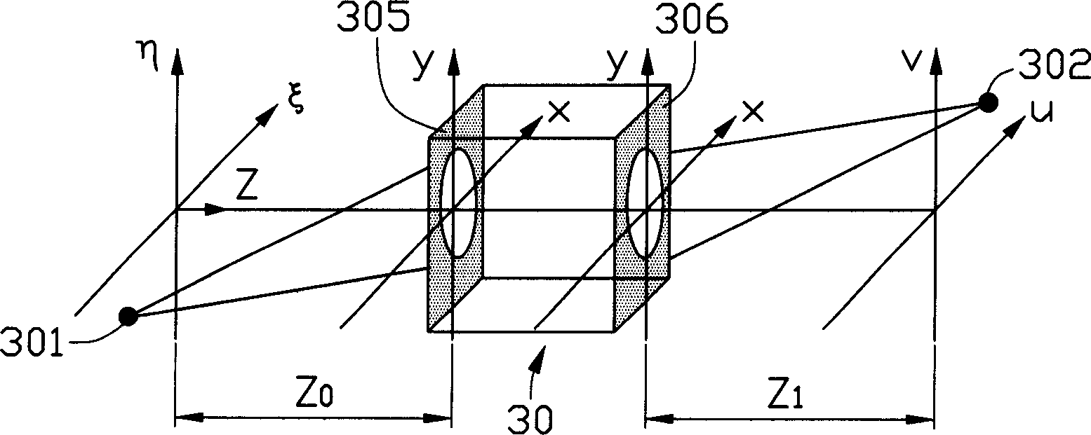
[0032] see figure 2 , is a schematic diagram of the optical system of a commonly used exposure machine. The light emitted by the light source 301 enters the optical system 30 of the exposure machine from the incident surface 305 of the optical system 30 , and then exits from the output surface 306 of the optical system 30 , and forms a projection 302 on the projection surface behind the optical system 30 . Z0 represents the distance between the light source 301 and the incident surface 305 of the optical system 30 , that is, the object distance; Z1 represents the distance between the projection 302 and the outgoing surface 306 of the optical system 30 , that is, the image distance.

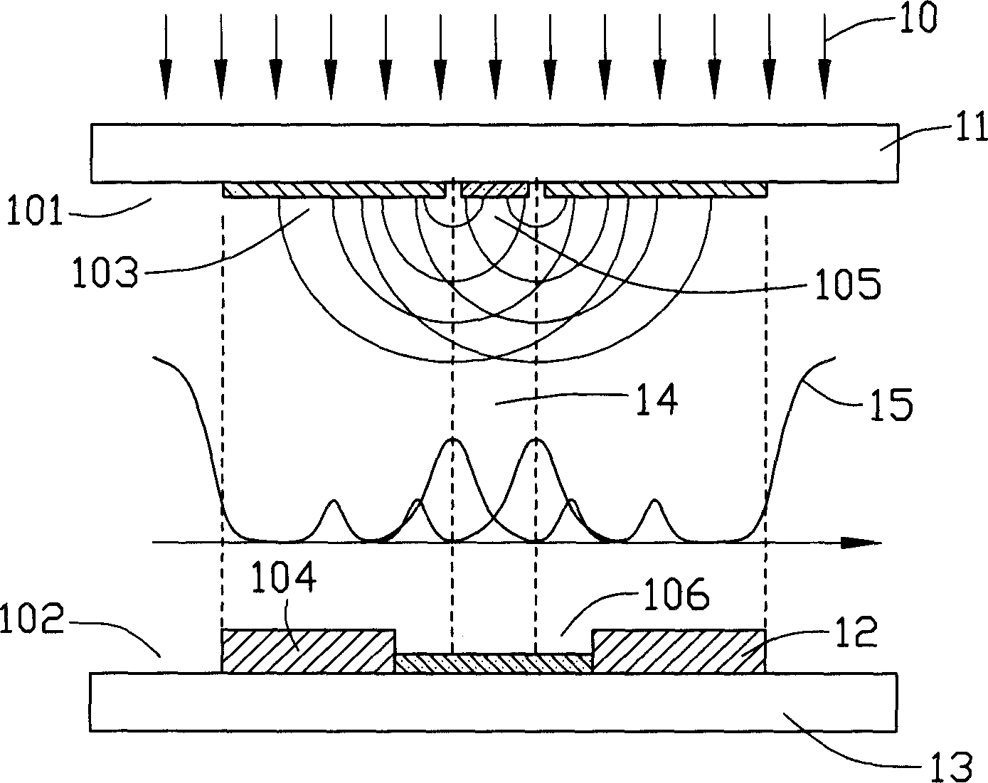
[0033] In the exposure process, among various factors affecting the exposure resolution, the influence of slit diffraction is more obvious....


PUM


Abstract

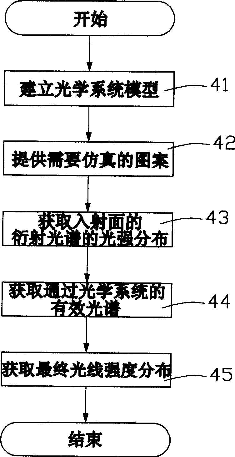
The simulating method of exposure system includes the following steps: establishing optical system model; initializing one data processing device; setting the relevant parameters of the optical system in the data processing device; providing pattern to be simulated; analyzing the pattern; analyzing the input pattern, and transforming the pattern to obtain the light strength distribution spectrum of the far field diffracted light in the incident plane of the optical system; multiplying the diffraction spectrum and the transfer function of the optical system to obtain the effective diffraction spectrum of the optical system; and performing corresponding inverse transformation of the effective diffraction spectrum to obtain the final light intensity distribution.

Description

【Technical field】 [0001] The invention relates to a simulation method and a simulation device, in particular to a simulation method and a simulation device of an exposure system. 【Background technique】 [0002] In the manufacturing process of semiconductor devices, liquid crystal display devices, etc., more exposure (Lithography) and development (Development) processes are required, but the process is usually more complicated and the yield rate is lower. In order to improve production yield, reduce cost, and simplify manufacturing process, the industry has proposed a slit pattern mask method. This method mainly uses the diffraction phenomenon that occurs when light passes through a slit whose size is close to the wavelength of the light. For a diffraction grating, on the projection surface behind the grating, even if the opaque part of the grating corresponds to the projection surface behind the grating, there will still be a certain amount of light, that is, the light inte...

Claims


Application Information

Patent Timeline
Patent Type & Authority Applications(China)
IPC IPC(8): G03F7/20G02F1/133H01L21/00G06F3/00G06T1/00
Inventor 赖建廷彭家鹏
Owner HONG FU JIN PRECISION IND (SHENZHEN) CO LTD
Learn More