

Laminate, printed wiring board and method for manufacturing them
A technology of laminates and metal layers, which is applied in the fields of printed circuit manufacturing, printed circuits, chemical instruments and methods, etc., and can solve the problem of low tolerance
- Summary
- Abstract
- Description
- Claims
- Application Information
AI Technical Summary
Problems solved by technology
Method used
Image

Examples
Embodiment 1~6
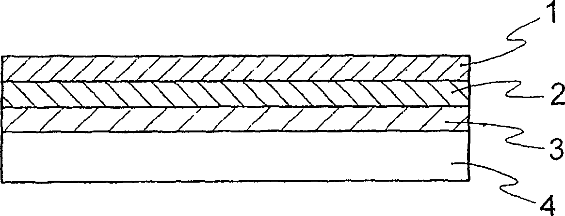
[0182] The polyimide film was prepared by coating one side of the non-thermoplastic polyimide film with a thickness of 25 μm prepared by the preparation method A, B or C by coating the polyamic acid solution prepared by the production method X or Y. The thickness of the thermoplastic polyimide layer is 3 μm.
[0183]Next, nickel was sputtered for 1 minute on the thermoplastic polyimide layer to form a nickel film with a thickness of 6 nm. Copper sputtering was continuously performed for 9 minutes to form a copper film with a thickness of 100 nm to obtain a metal layer / polyimide thin film laminated body. On the obtained sputtered film, a copper layer having a thickness of 18 μm was formed by electrolytic plating. The adhesive strength at room temperature, the adhesive strength after the pressure retort test, and the decontamination resistance of the laminate were measured. The results are shown in Table 2.
[0184] Example
[0185] From the results, it can be seen ...
Embodiment 7~14
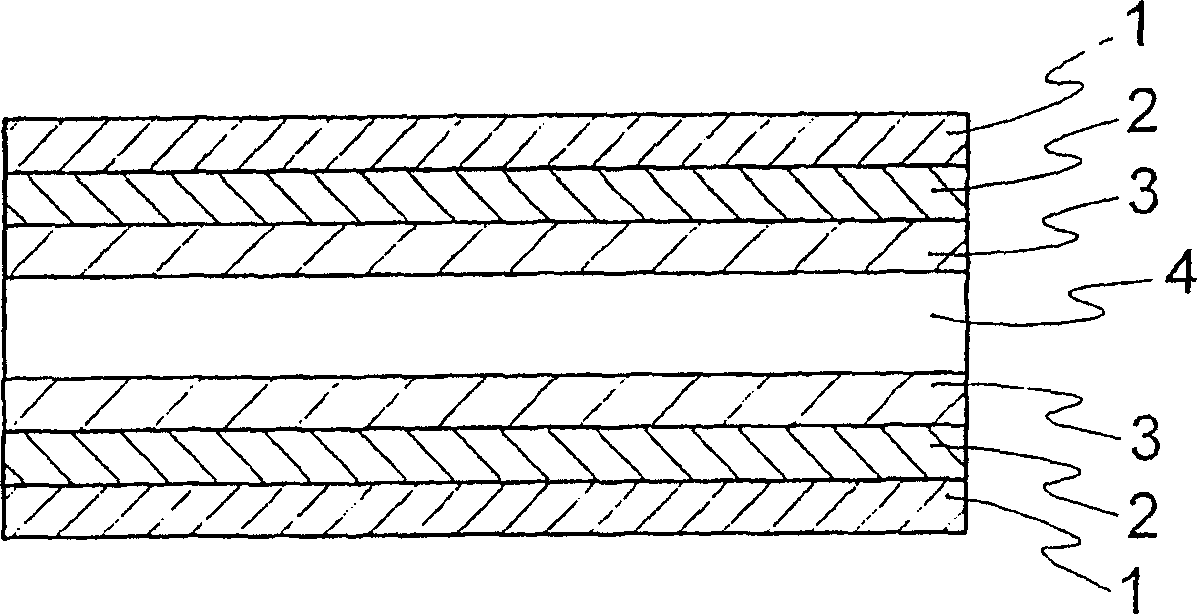
[0187] The polyamic acid solution prepared by the production method Y was coated on both sides of the non-thermoplastic polyimide film with a thickness of 25 μm prepared by the production method C to prepare samples forming thermoplastic polyimide layers with different thicknesses. Nickel was sputtered for 1 minute on this thin film to form a nickel film with a thickness of 6 nm. Copper sputtering was continuously performed for 9 minutes to form a copper film with a thickness of 100 nm to obtain a metal layer / polyimide thin film laminated body. Using the obtained sputtered film as a power supply layer, a copper layer having a thickness of 18 μm was formed by electrolytic plating. The adhesive strength at room temperature, the adhesive strength after the pressure cooking test, the decontamination resistance, and the thermal expansion coefficient of the obtained laminate were measured. The results are shown in Table 3. Here, regarding the thermal expansion rate, the thermal ex...
Embodiment 15~22
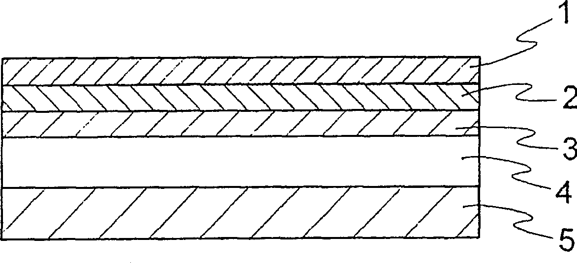
[0191] On both sides of the non-thermoplastic polyimide film with a thickness of 7.5 μm, 12.5 μm, 25 μm and 50 μm prepared by the preparation method C, the polyamic acid solution prepared by the preparation method Y is coated, and the formation of 1 μm, 5 μm and 10 μm is made by this method The thickness of the thermoplastic polyimide laminated body.
[0192] Nickel was sputtered for 1 minute on this thin film to form a nickel film with a thickness of 6 nm. Copper sputtering was continuously performed for 9 minutes to form a copper film with a thickness of 100 nm to obtain a metal layer / polyimide thin film laminated body. Using the obtained sputtered film as a power supply layer, a copper layer having a thickness of 5 nm was formed by electrolytic plating. The adhesive strength at room temperature, the adhesive strength after the pressure cooking test, the decontamination resistance, and the thermal expansion coefficient of the obtained laminate were measured. The results ar...
PUM
| Property | Measurement | Unit |
|---|---|---|
| thickness | aaaaa | aaaaa |
| thickness | aaaaa | aaaaa |
| thickness | aaaaa | aaaaa |
Abstract
Description
Claims
Application Information