Manufacturing method of grating oxide film

A gate oxide film and manufacturing method technology, applied in semiconductor/solid-state device manufacturing, electrical components, circuits, etc., can solve the problems of difficulty in oxide film 6a and reduced oxidation efficiency, and achieve the effect of improving oxidation efficiency

Inactive Publication Date: 2006-01-18
YAMAHA CORP
View PDF3 Cites 7 Cited by
  • Summary
  • Abstract
  • Description
  • Claims
  • Application Information

AI Technical Summary

Problems solved by technology

Therefore, the oxidation efficiency in the element port 2a will decrease, and it will be difficult to obtain the oxide film 6a having a sufficient thickness compared to the oxide film 6b.

Method used


Image

  • Manufacturing method of grating oxide film
  • Manufacturing method of grating oxide film
  • Manufacturing method of grating oxide film

Examples


no. 1 example

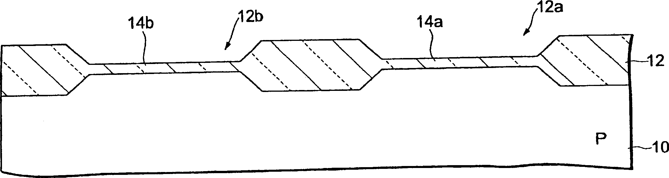
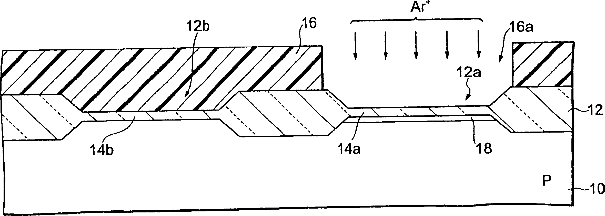
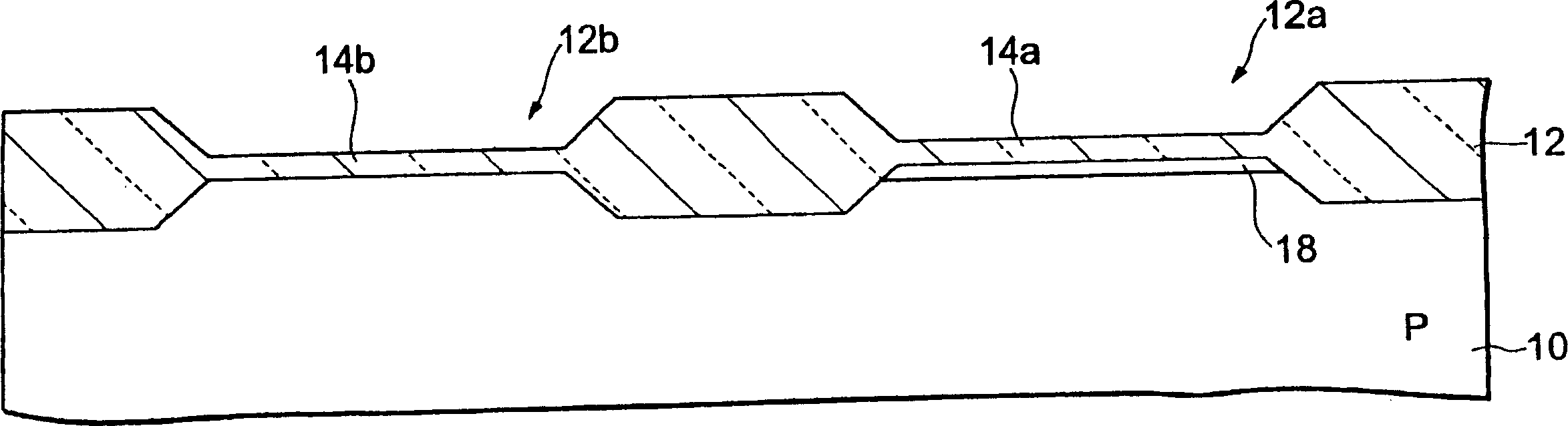
[0084] According to the first embodiment of the present invention, under one of the following conditions by figure 2 The ion implantation process shown in forms the ion implantation layer 18 or 18a, that is, under the acceleration voltage of 20-50keV, the 14 to 2×10 16 ions / cm 2 Argon ions were implanted at a dose of 15-25keV at an accelerating voltage of 6×10 14 to 1×10 15 ions / cm 2 The dose of fluorine ions is implanted, and argon ions or fluorine ions are implanted in two steps; thus, the ion implantation layer 18 or 18a is formed from a relatively deep region of the surface of the silicon substrate. Therefore, when Figure 4 When cleaning with an etching effect is performed in the illustrated cleaning process, the ion-implanted layer 18 or 18a will not be removed by the etching effect because the ion-implanted layer 18 or 18a is formed from a relatively deep region of the silicon substrate surface. Thereafter, when performing Figure 5 During the thermal oxidation ...


PUM


Abstract

After forming a field insulating film 12 on a substrate, sacrificing or gate oxidation films are formed as oxidation films 14 a and 14 b. An ion implantation layer 18 is formed by one or plurality of implantation process of argon (or fluoride) ion in an element hole 12 a using a resist layer 16 as a mask via the oxidation film 14 a. When the oxidation films 14 a and 14 b are used as sacrificing oxidation films, gate oxidation films are formed in the element holes 12 a and 12 b after removing the resist film 16 and the oxidation films 14 a and 14 b. When the oxidation films 14 a and 14 b are used as gate oxidation films, the oxidation films are once thinned by etching and then thickened after removing the resist layer 16. The gate oxidation film 14 a is thicker than the gate oxidation film 14 b by forming the ion implantation layer 18.

Description

technical field [0001] The present invention relates to a method of manufacturing a gate oxide film suitable for use in manufacturing MOS type ICs and the like, and more particularly to a method of manufacturing a plurality of gate oxide films having thicknesses different from each other formed in one thermal oxidation process. Background technique [0002] Conventionally, when manufacturing a MOS type IC or the like, a plurality of MOS type transistors having different thicknesses from each other are formed on a semiconductor substrate. In addition to this technique involved, various types of methods have been proposed in which a plurality of gate oxide films having thicknesses different from each other are formed in one thermal oxidation process. Figure 16 to Figure 18 An example of a gate oxide film forming method is shown. The entire contents of Japanese Laid-Open Patent No. 2000-195968 are incorporated herein as reference for details of the gate oxide film forming meth...

Claims


Application Information

Patent Timeline
Patent Type & Authority Applications(China)
IPC IPC(8): H01L21/8234
Inventor 高见秀诚
Owner YAMAHA CORP
Why Eureka
Try Eureka