Light-emitting diode

A technology of light-emitting diodes and light-emitting layers, which is applied in the direction of electrical components, electric solid-state devices, circuits, etc.

Inactive Publication Date: 2006-02-15
SANYO ELECTRIC CO LTD +1
View PDF0 Cites 4 Cited by
  • Summary
  • Abstract
  • Description
  • Claims
  • Application Information

AI Technical Summary

Problems solved by technology

[0007] Also, in Patent Publication 1, it can be said that it is impossible to apply this light-emitting diode to a light-emitting diode having a cup-shaped lead frame from the viewpoint of manufacturing engineering

Method used


Image

  • Light-emitting diode
  • Light-emitting diode
  • Light-emitting diode

Examples


Embodiment Construction

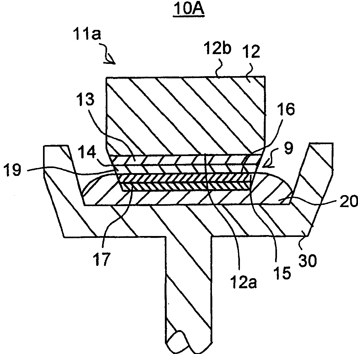
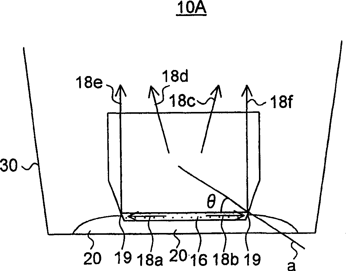
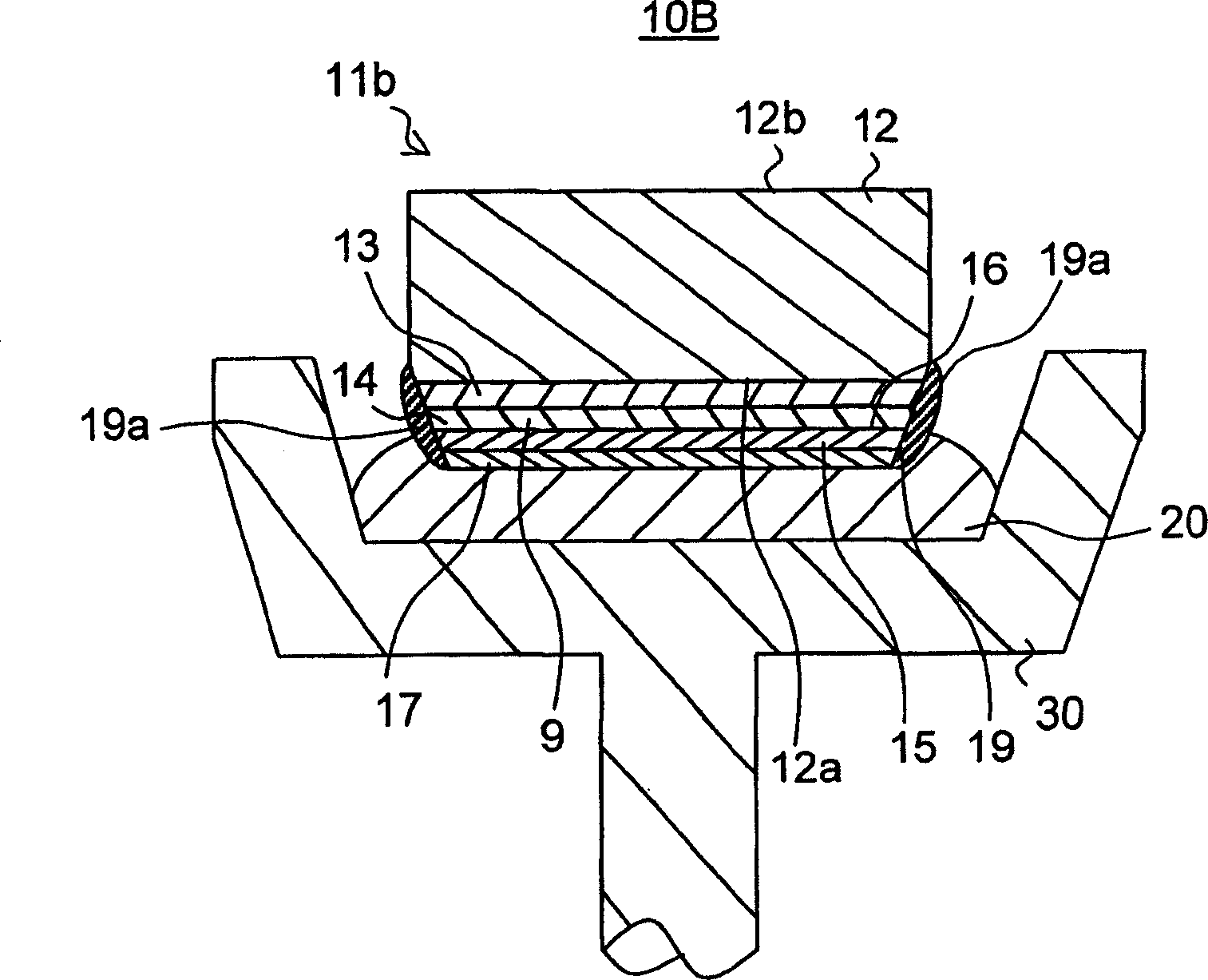
[0058] Embodiments of the present invention will be described below with reference to the accompanying drawings. For clarity, with the aforementioned Image 6 with 7 Similar parts are denoted by the same reference numerals. It should be understood that the present invention may be practiced in any manner other than as specifically shown in the drawings. figure 1 is a sectional view showing a light emitting diode according to a first embodiment of the present invention.

[0059] The light emitting diode 10A has an LED chip 11 a disposed on top of a cup-shaped lead frame 30 . The LED chip 11 a has a translucent substrate 12 formed of insulating sapphire, on a first surface 12 a of the sapphire substrate 12 a semiconductor layer 9 is formed via a buffer layer 13 . The semiconductor layer 9 is composed of a first conductivity type semiconductor layer 14 and a second conductivity type semiconductor layer 15, wherein the first conductivity type semiconductor layer 14 is formed b...


PUM


Abstract

A light emitting diode (10A) produced by securing a light emitting element (11a) to a lead frame (30) with a conductive adhesive material (20) is disclosed wherein the light emitting element (11a) comprises a semiconductor layer (9) including a light emitting layer (16) which is formed on a first surface (12a) of a translucent substrate (12) whose second surface (12b) is opposite to the first surface (12a) and serves as an emission observing surface. The semiconductor layer (9) has a side face (19) inclined to the first surface (12a) and the angle theta between a normal (a) to the inclined side face (19) and a crystal plane for growing the light emitting layer (16) is set such that the light emitted from the light emitting layer (16) is totally reflected toward the translucent substrate (12).

Description

technical field [0001] The invention relates to a light emitting diode having a light emitting element consisting of a semiconductor layer placed on top of a translucent substrate. Background technique [0002] One of the challenges with light emitting devices such as blue light emitting diodes and blue laser diodes is how to increase the efficiency of light extraction from the light emitting element. In particular, the luminous efficiency of white light-emitting diodes is increasing every year, almost doubling every two years. Even with this rapid improvement, it can be said that it will take a few more years to catch up with the luminous efficiency of 60 lm / W of fluorescent lamps generally used at home. [0003] On the other hand, in light-emitting diodes currently under development, approximately 80% of the light generated is wasted. Part of the light that does not exit the light-emitting element is repeatedly reflected in the element, and is converted into heat energy ...

Claims


Application Information

Patent Timeline
Patent Type & Authority Applications(China)
IPC IPC(8): H01L33/00H01L33/20H01L33/38
CPCH01L33/20H01L33/382H01L24/32H01L2224/48091H01L2224/48247H01L2224/73265H01L2924/15787H01L2924/12041H01L2924/00014H01L2924/00
Inventor 松下保彦
Owner SANYO ELECTRIC CO LTD
Why Eureka
Try Eureka