Polymeric optical device structures having controlled topographic and refractive index profiles

A technology of optical devices and refractive index, applied in optical components, optics, instruments, etc., can solve problems such as roughness

Inactive Publication Date: 2006-02-22
GENERAL ELECTRIC CO
View PDF0 Cites 6 Cited by
  • Summary
  • Abstract
  • Description
  • Claims
  • Application Information

AI Technical Summary

Problems solved by technology

Another problem encountered with planar polymer waveguides is the necessity to have smooth edges on the waveguide structure to limit optical transmission losses
We believe that determining the waveguide structure using conventional reactive ion etching techniques will produce edges that will be too rough for single-mode light transmission

Method used


Image

  • Polymeric optical device structures having controlled topographic and refractive index profiles
  • Polymeric optical device structures having controlled topographic and refractive index profiles
  • Polymeric optical device structures having controlled topographic and refractive index profiles

Examples


Embodiment 1

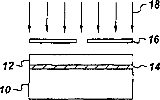
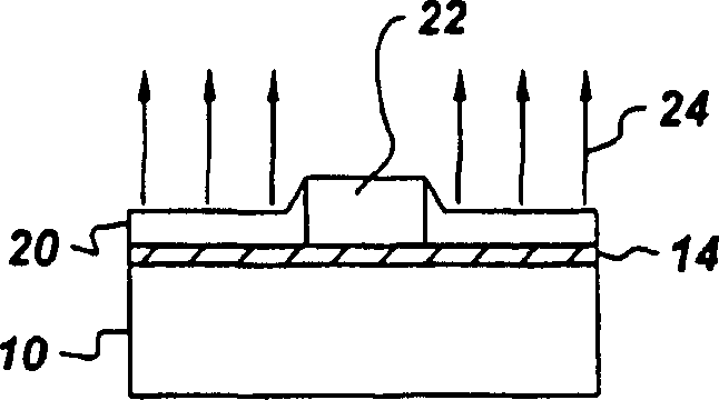
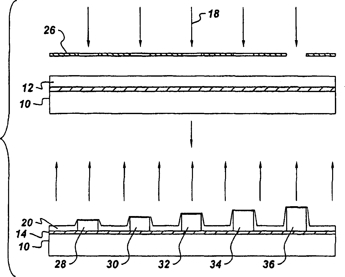
[0050] This example describes the use of UV radiation to prepare TM Surface topography of polymer composites of 9371 polycarbonate (available from Bayer Company) and CY 179.

[0051] Preparation contains about 50 parts by weight of Apec TM A mixture of polycarbonate, about 50 parts by weight of CY 179, 1 part by weight of Cyracure UVI-6976 photocatalyst, 150 parts by weight of anisole and 50 parts by weight of cyclopentanone. A 50 micron thick film was prepared on a glass substrate by spin coating the material and partially curing it at 90°C for 20 minutes to remove the solvent. Image exposure using chrome patterned on a quartz plate and patterned on a polycarbonate / epoxy film. Exposure was performed for 30 seconds using a Karl Suss contact printer. After exposure, the samples were baked on a hot plate at 200°C for 1 hour. Surface profile measurements of the resulting surface topography showed a step of approximately 23 microns between the underlying unexposed film surfac...


PUM

PropertyMeasurementUnit
sizeaaaaaaaaaa
sizeaaaaaaaaaa
sizeaaaaaaaaaa

Abstract

An optical device structure (22) comprising a substrate (10) and at least one topographic feature. The topographic feature comprises a polymeric composite material formed from a polymerizable binder and an uncured monomer. The topographic feature has a controlled topographic profile and a controlled refractive index across the topolografic feature. The optical device structure may be a multimode waveguide device, a single mode waveguide device, an optical data storage device, thermo-optic switches, a lens, or microelectronic mechanical system.

Description

Background of the invention [0001] The present invention relates to optical device structures comprising polymer composites. More particularly, the present invention relates to a topological feature forming an optical device structure. The present invention can be used to form optical device structures including clad layers and core layers. [0002] Modern high-speed communication systems increasingly use optical fibers to transmit and receive high bandwidth data. The excellent properties of polymer optical fibers in terms of flexibility, ease of handling, and installation are important drivers for their implementation in high-bandwidth, short-range data transmission applications, such as fibers for home, local area networks, and automated information, diagnostic, and entertainment systems . [0003] In any type of optical communication system, different discrete components need to be interconnected. These components may include devices such as lasers, detectors, fiber mod...

Claims


Application Information

Patent Timeline
Patent Type & Authority Applications(China)
IPC IPC(8): G02B6/12G02B3/00G02B6/138
CPCG02B6/138G02B3/0056G02B3/0012G02B6/12
Inventor 施旻宜托马斯·B·戈克齐卡
Owner GENERAL ELECTRIC CO
Why Eureka
Try Eureka