
Trench MOSFET technology for DC-DC converter applications
A DC converter and slot technology, which is applied in the field of 7] to achieve the effect of reducing the start-up resistance, the start-up resistance and the improvement of the current-carrying capacity characteristics.
- Summary
- Abstract
- Description
- Claims
- Application Information
AI Technical Summary
Problems solved by technology
Method used
Image

Examples
Embodiment Construction
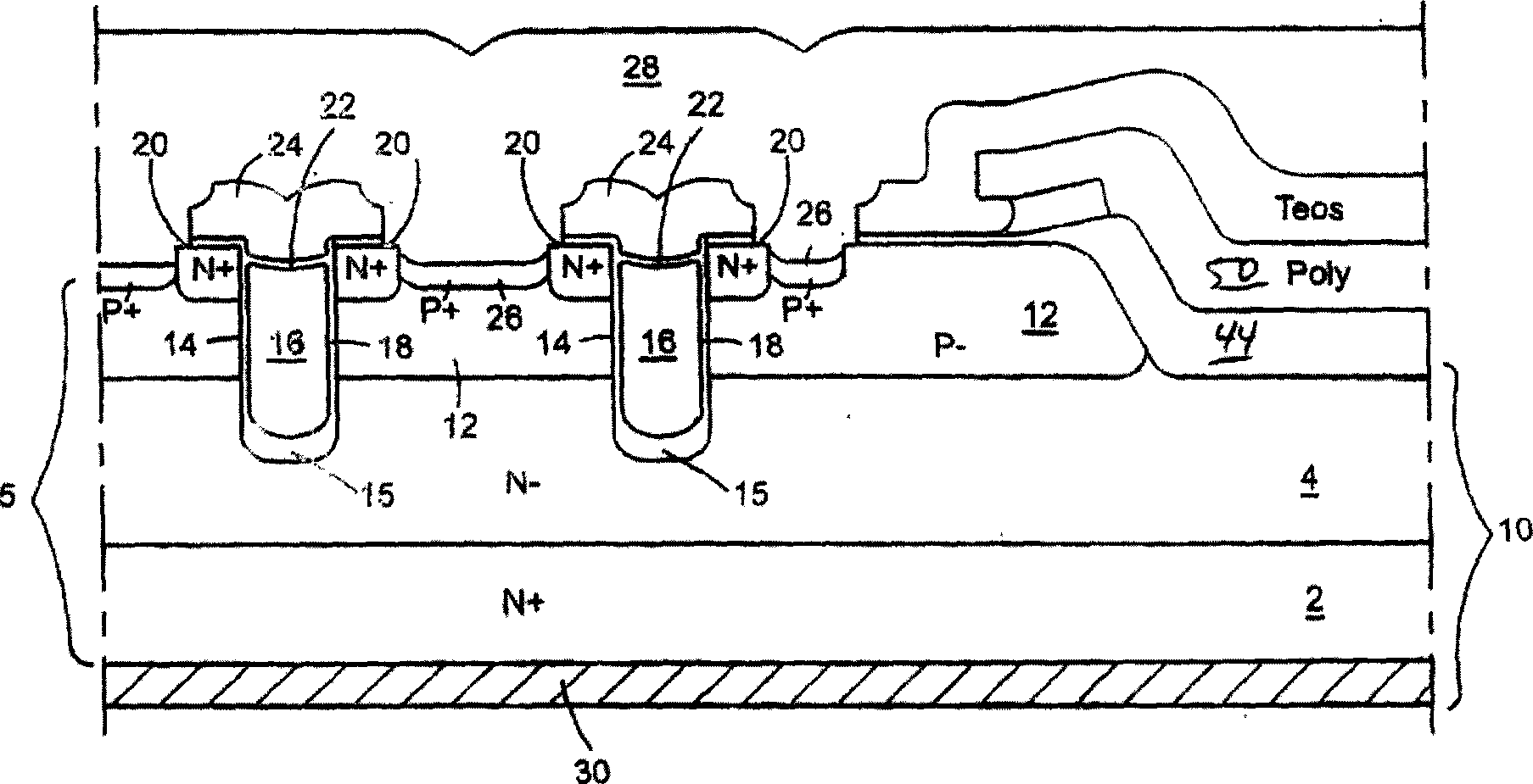
[0020] exist figure 1 Here, the semiconductor device of the present invention is formed in a silicon wafer 5 comprising a drain region 10 of a first conductivity type and a channel region 12 slightly doped with a dopant of a conductivity type opposite to that of the drain region 10. The semiconductor device of the present invention includes multiple trenches 14 extending from the top surface of the silicon wafer 5 to the drain region 10, where the trenches 14 are formed of a gate electrode 16 using a conductive material such as doped polysilicon. The gate electrode 16 is electrically insulated from the channel region 12 by the oxide layer 18 . An oxide layer 18 grows on both side walls of each trench 14, and care must be taken to form a thicker oxide layer 15 at the bottom of each trench.
[0021] The semiconductor device of the present invention further includes a self-aligned source region 20 disposed on opposite sides of each trench 14 and extending to a predetermined dept...
PUM
 Abstract
Description
Claims
Application Information