Method for preparing nano phase transformation memory unit capable of reducing write-operation current
A memory cell, nano-phase technology, applied in the field of microelectronics, can solve the problems of high power consumption of devices and large write operation current, and achieve the effect of solving high power consumption of devices
- Summary
- Abstract
- Description
- Claims
- Application Information
AI Technical Summary
Problems solved by technology
Method used
Image

Examples
Embodiment 1
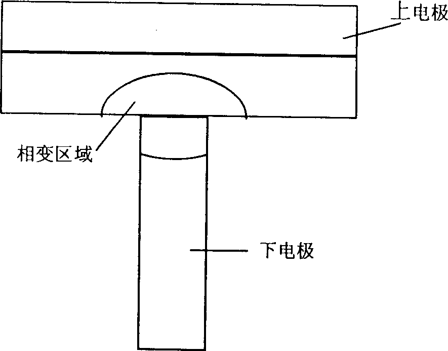
[0037] The preparation method of the memory cell structure proposed by the present invention is specifically as follows in conjunction with the accompanying drawings:
[0038] a. Choose a low-resistance type (111) silicon wafer, first use acetone to ultrasonically remove the surface organic matter, and then use concentrated H 2 SO 4 :H 2 o 2 : 1:1 heating to 100±10 degrees for about 5 minutes, then rinse and dry with deionized water, then put the silicon wafer into 10:1 water:HF solution for 20±2 seconds to remove surface oxide , then rinse and dry with deionized water, and then put the silicon wafer into NH 4 OH:H 2 o 2 :H 2 O=1:2:5 volume ratio of No. I solution was boiled for 5 minutes, then rinsed with deionized water and dried, and then put the silicon wafer into HCL:H 2 o 2 :H 2 The No. II liquid with a volume ratio of O=1:2:8 was boiled for 10 minutes, then rinsed and dried with deionized water.
[0039] b. Deposit the lower electrode material 2, such as TiN, ...
Embodiment 2
[0048] a. Choose a low-resistance type (111) silicon wafer, first use acetone to ultrasonically remove the surface organic matter, and then use concentrated H 2 SO 4 :H 2 o 2 : 1:1 heating to 100±10 degrees for about 5 minutes, then rinse and dry with deionized water, then put the silicon wafer into 10:1 water:HF solution for 20±2 seconds to remove surface oxide , then rinse and dry with deionized water, and then put the silicon wafer into NH 4 OH:H 2 o 2 :H 2 O=1:2:5 volume ratio of No. I solution was boiled for 5 minutes, then rinsed with deionized water and dried, and then put the silicon wafer into HCL:H 2 o 2 :H 2 The No. II liquid with a volume ratio of O=1:2:8 was boiled for 10 minutes, then rinsed and dried with deionized water.
[0049] b. Deposit the lower electrode material 2 on the cleaned silicon wafer, such as TiN, W, etc.; ( Figure 4b ).
[0050] c. Depositing an Al layer 4 on the lower electrode material; ( Figure 5b ).
[0051] d. Anodized porou...
Embodiment 3
[0057] a. Choose a low-resistance type (111) silicon wafer, first use acetone to ultrasonically remove the surface organic matter, and then use concentrated H 2 SO 4 :H 2 o 2 : 1:1 heating to 100±10 degrees for about 5 minutes, then rinse and dry with deionized water, then put the silicon wafer into 10:1 water:HF solution for 20±2 seconds to remove surface oxide , then rinse and dry with deionized water, and then put the silicon wafer into NH 4 OH:H 2 o 2 :H 2 O=1:2:5 volume ratio of No. I solution was boiled for 5 minutes, then rinsed with deionized water and dried, and then put the silicon wafer into HCL:H 2 o 2 :H 2 The No. II liquid with a volume ratio of O=1:2:8 was boiled for 10 minutes, then rinsed and dried with deionized water.
[0058] b. Deposit the lower electrode material 2 on the cleaned silicon wafer, such as TiN, W, etc.; ( Figure 4b ).
[0059] c. Depositing an Al layer 4 on the lower electrode material; ( Figure 5b ).
[0060] d. Anodized porou...
PUM
 Abstract
Description
Claims
Application Information
 - Generate Ideas
- Intellectual Property
- Life Sciences
- Materials
- Tech Scout
- Unparalleled Data Quality
- Higher Quality Content
- 60% Fewer Hallucinations
Browse by: Latest US Patents, China's latest patents, Technical Efficacy Thesaurus, Application Domain, Technology Topic, Popular Technical Reports.
© 2025 PatSnap. All rights reserved.Legal|Privacy policy|Modern Slavery Act Transparency Statement|Sitemap|About US| Contact US: help@patsnap.com