Dynamic random access memory unit and its array, and Method of making the same

A dynamic random access and memory cell technology, applied in semiconductor/solid-state device manufacturing, electrical components, transistors, etc., can solve problems such as increasing the surface area of ​​capacitors, and achieve the effect of quality improvement

Active Publication Date: 2006-05-03
PROMOS TECH INC
View PDF0 Cites 4 Cited by
  • Summary
  • Abstract
  • Description
  • Claims
  • Application Information

AI Technical Summary

Problems solved by technology

[0004] In view of this, the object of the present invention is to provide a dynamic random access memory cell, which has a capacitor formed on the sidewall of the semiconductor pillar, to solve the existing problem of filling the trench, and to increase the surface area of ​​the capacitor

Method used


Image

  • Dynamic random access memory unit and its array, and Method of making the same
  • Dynamic random access memory unit and its array, and Method of making the same
  • Dynamic random access memory unit and its array, and Method of making the same

Examples


Embodiment Construction

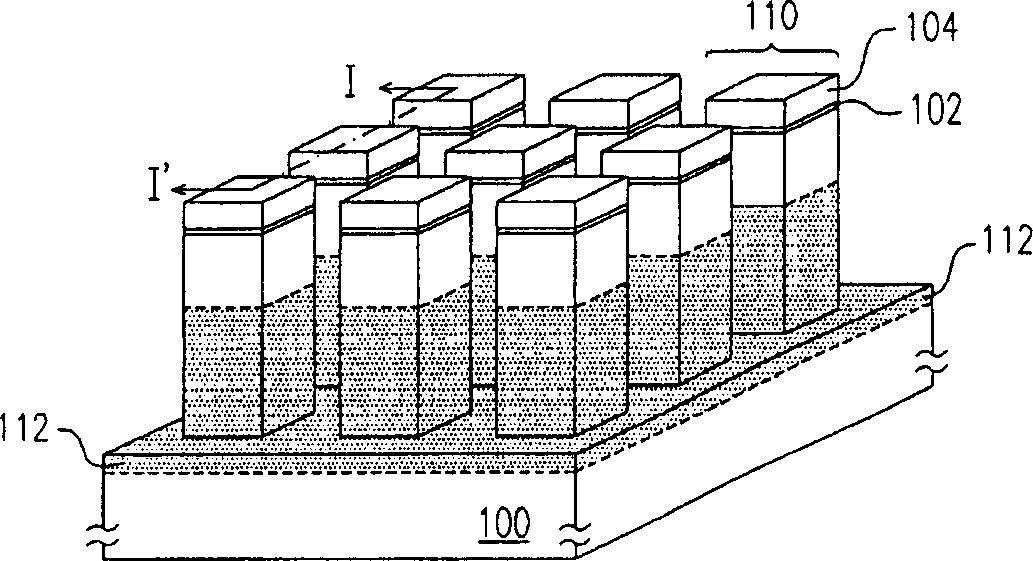
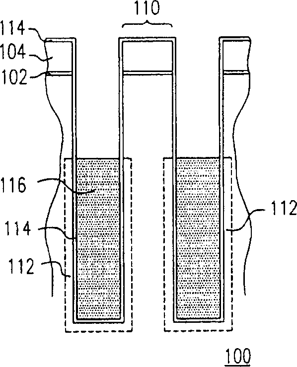
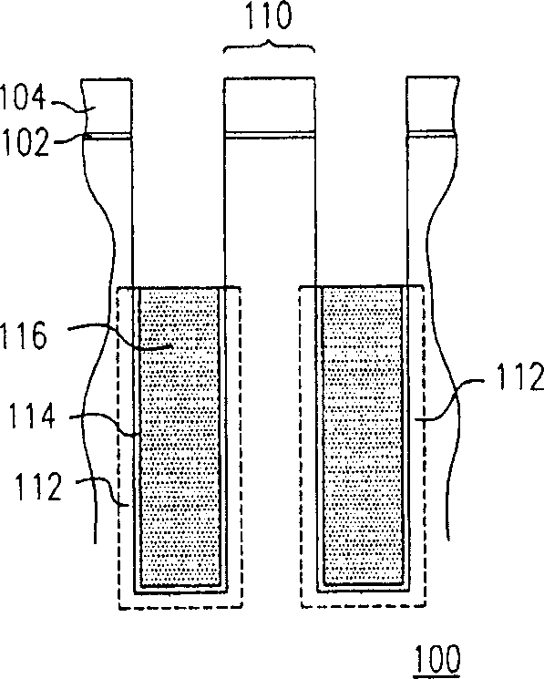
[0030] figure 1 perspective view clearly showing the dynamic random access memory array, Figure 2 to Figure 11 , Figure 13 to Figure 15 as well as Figure 18 (a) is along the figure 1 The cross-sectional schematic diagram of the I-I' line in Figure 18 (b) is another schematic sectional view, and Figure 12 , Figure 16 and Figure 17 All are top views.

[0031] More specifically, Figure 1 to Figure 7 Shown is a schematic of the fabrication process for forming capacitors for dynamic random access memory arrays, Figure 8 to Figure 14 Illustrated is a schematic of the fabrication flow of transistors forming a dynamic random access memory array, and Figure 15 to Figure 18 Shown are subsequent steps, including bit line and word line manufacturing methods.

[0032]

[0033] First, please refer to figure 1 , providing a semiconductor substrate 100 made of, for example, lightly doped P-type single crystal silicon, and forming a pad oxide layer 102 and a patterned...


PUM


Abstract

The invention relates to a dynamic random access memory unit and its array and the method for making the array. The dynamic random access memory unit comprises a semi-conducting column on the base, a capacitor on the side lower part of the semi-conducting column and a vertical crystal pipe on the side upper part of the semi-conducting column. The capacitor comprises: a first plate on the side lower part of the semi-conducting column, a second plate around the first pate as upper electrode, a third plate around the second pate and a dielectric layer which divides the second plate and the first and third plates. The third plate is connected with the first plate to form lower electrode. The invention also provides the method for making the dynamic random access memory unit and its array.

Description

technical field [0001] The present invention relates to a semiconductor device, and in particular to a storage unit and an array structure of a DRAM, and a manufacturing process of the DRAM array. DRAM cells feature capacitors with high capacitance. Background technique [0002] In the semiconductor industry, DRAM is one of the most important integrated circuits, so it stimulates continuous research and development. Increasing the storage capacity, improving the writing and reading speed, and reducing the device area size of the DRAM cell are the goals of continuous efforts. In general, a DRAM cell includes a transistor and a capacitor operated by the transistor. Traditionally, the design of DRAM cells can be divided into three types, namely planar, stacked capacitor and trench. In a planar design, the transistors and capacitors of the memory cell are fabricated with planar components. In a stacked capacitor design, the capacitor of the memory cell is placed above the tr...

Claims


Application Information

Patent Timeline
Patent Type & Authority Applications(China)
IPC IPC(8): H01L27/108H01L21/8242
Inventor 王廷熏
Owner PROMOS TECH INC
Why Eureka
Try Eureka