Interspace technical method for implementing copper connecting lines in semiconductor device

A process method and semiconductor technology, applied in the fields of semiconductor/solid-state device manufacturing, electrical components, circuits, etc., can solve the problems of slow circuit running speed, large parasitic capacitance between copper connections, affecting circuit running speed, etc.

Active Publication Date: 2006-07-05
SHANGHAI HUAHONG GRACE SEMICON MFG CORP
View PDF0 Cites 3 Cited by
  • Summary
  • Abstract
  • Description
  • Claims
  • Application Information

AI Technical Summary

Problems solved by technology

[0002] At present, in the semiconductor device manufacturing process, when implementing the copper wiring process, it is necessary to fill some kind of dielectric (OXIDE, FSG, etc.) in the la

Method used


Image

  • Interspace technical method for implementing copper connecting lines in semiconductor device
  • Interspace technical method for implementing copper connecting lines in semiconductor device
  • Interspace technical method for implementing copper connecting lines in semiconductor device

Examples


Embodiment Construction

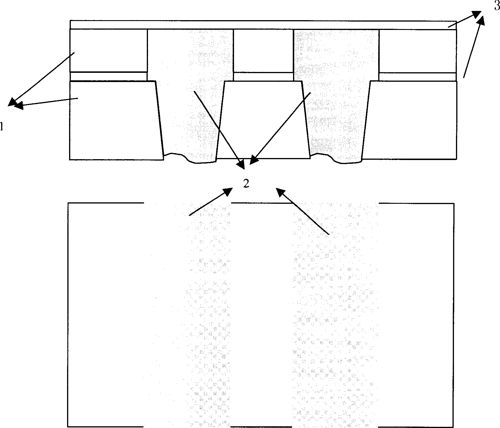
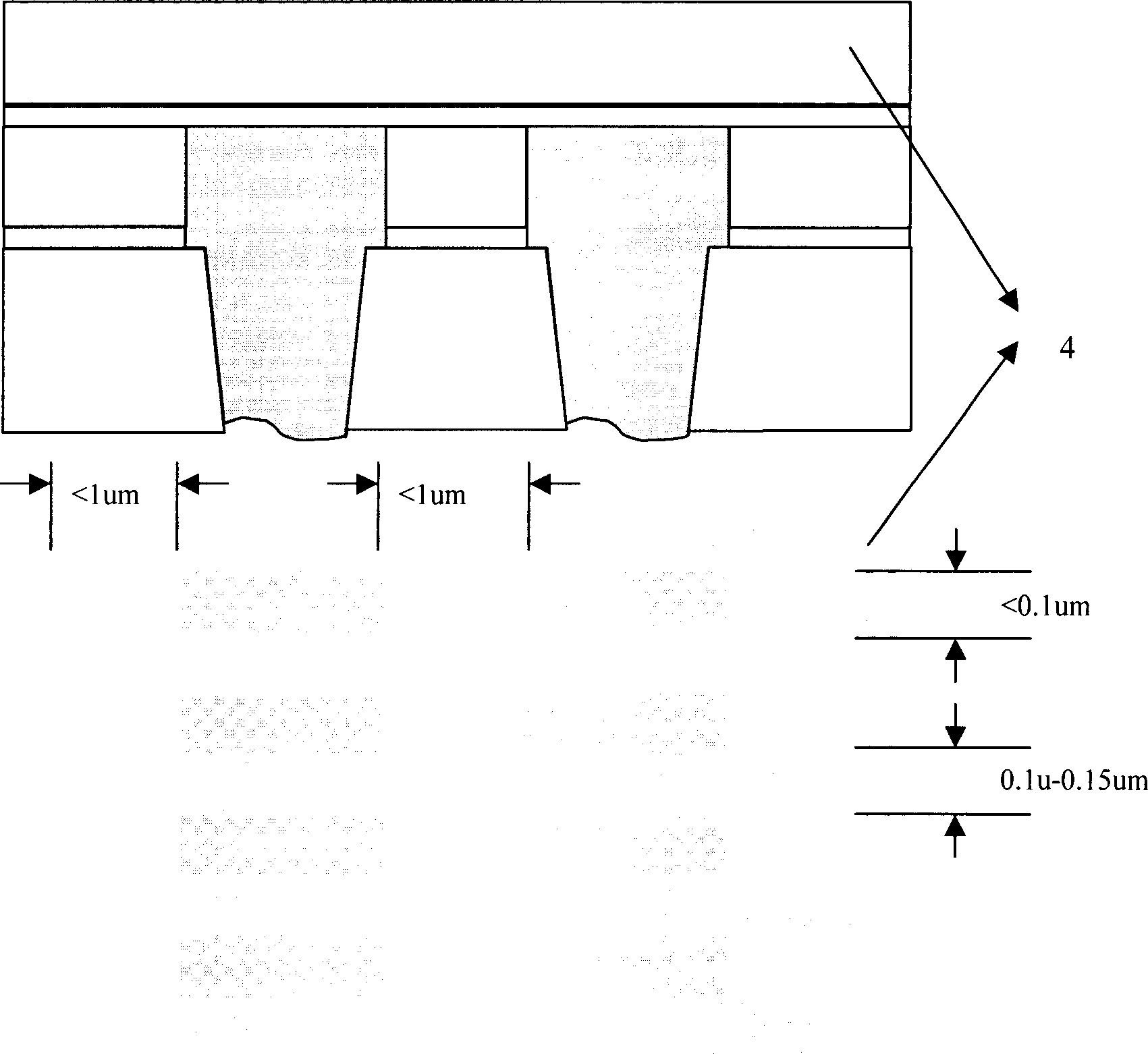
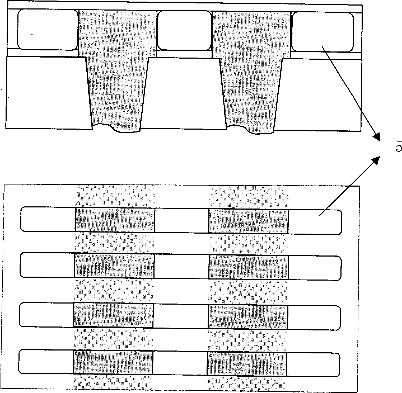
[0012] The process method of implementing copper wiring in semiconductor devices of the present invention is that the last process of making one layer of through holes and copper wiring is copper CMP, and thereafter, a layer of SiN (silicon nitride) is grown. Coat the photoresist on the chip, and do a photolithography with a photolithography plate made by the following method. The photolithography board can be produced according to the pattern of the lower layer copper wire, or can be manually drawn by the layout designer according to the actual situation. The pattern of the photolithography plate requires many small slits along the adjacent copper wires with a spacing of less than 1um and perpendicular to the direction of the copper wires. The size of the slits is less than 0.1um, and the distance between the slits is 0.1-0.15um.

[0013] After this photolithography, apply a dry etching process to etch off the upper layer of SiN and strip off the photoresist. Then use the is...


PUM


Abstract

After procedure of preparing a layer of through hole and copper connecting line, a layer of silicon is developed. Coating photoresist on the base plate, the method carries out photo etching by using a specific photo etching plate. Then, using dry etch technique graves out silicon at upper layer, and removes photoresist. Using isotropic dry etch technique graves out medium in gap and between copper wires under silicon. Using poor space-filling USG seals silicon opening. Medium layer in up level is deposited to start preparation of through hole and copper connecting line. The invention reduces parasitic capacitance between copper wires in transverse direction in order to reduce influence on operation speed of circuit.

Description

technical field [0001] The invention relates to a process method in the manufacture of a semiconductor chip, in particular to a method for implementing a copper connection gap process. Background technique [0002] At present, in the semiconductor device manufacturing process, when implementing the copper wiring process, it is necessary to fill some kind of dielectric (OXIDE, FSG, etc.) in the lateral gap of the copper wiring, which will make the parasitic capacitance between the copper wiring larger and affect The speed at which the circuit operates makes the circuit operate slower. Contents of the invention [0003] The technical problem to be solved by the present invention is to provide a process method for implementing copper wiring in a semiconductor device, which can reduce the parasitic capacitance between the copper wires laterally, so as to reduce the influence on the circuit running speed. [0004] In order to solve the above-mentioned technical problems, the p...

Claims


Application Information

Patent Timeline
IPC IPC(8): H01L21/768H01L21/3205H01L21/3213
Inventor 张宜高峰
Owner SHANGHAI HUAHONG GRACE SEMICON MFG CORP
Why Eureka
Try Eureka