Field emission display device in separated structure

A field emission and display device technology, used in image/graphic display tubes, instruments, optics, etc., can solve the problems of complex preparation process, restrict the promotion and application of surface conduction electron emission display, and achieve the effect of reducing technology and technology

Inactive Publication Date: 2006-07-19
SHAANXI UNIV OF SCI & TECH
View PDF0 Cites 43 Cited by
  • Summary
  • Abstract
  • Description
  • Claims
  • Application Information

AI Technical Summary

Problems solved by technology

However, the preparation process of nano-slits is not only complicated, but also has certain technical difficulties, which largely restricts the promotion and application of surface conduction electron emission displays; only when nanoscience and semiconductor technology develop to a certain level, this problem can be solved. solve

Method used


Image

  • Field emission display device in separated structure

Examples


Embodiment Construction

[0009] The present invention will be described in further detail below in conjunction with the accompanying drawings.

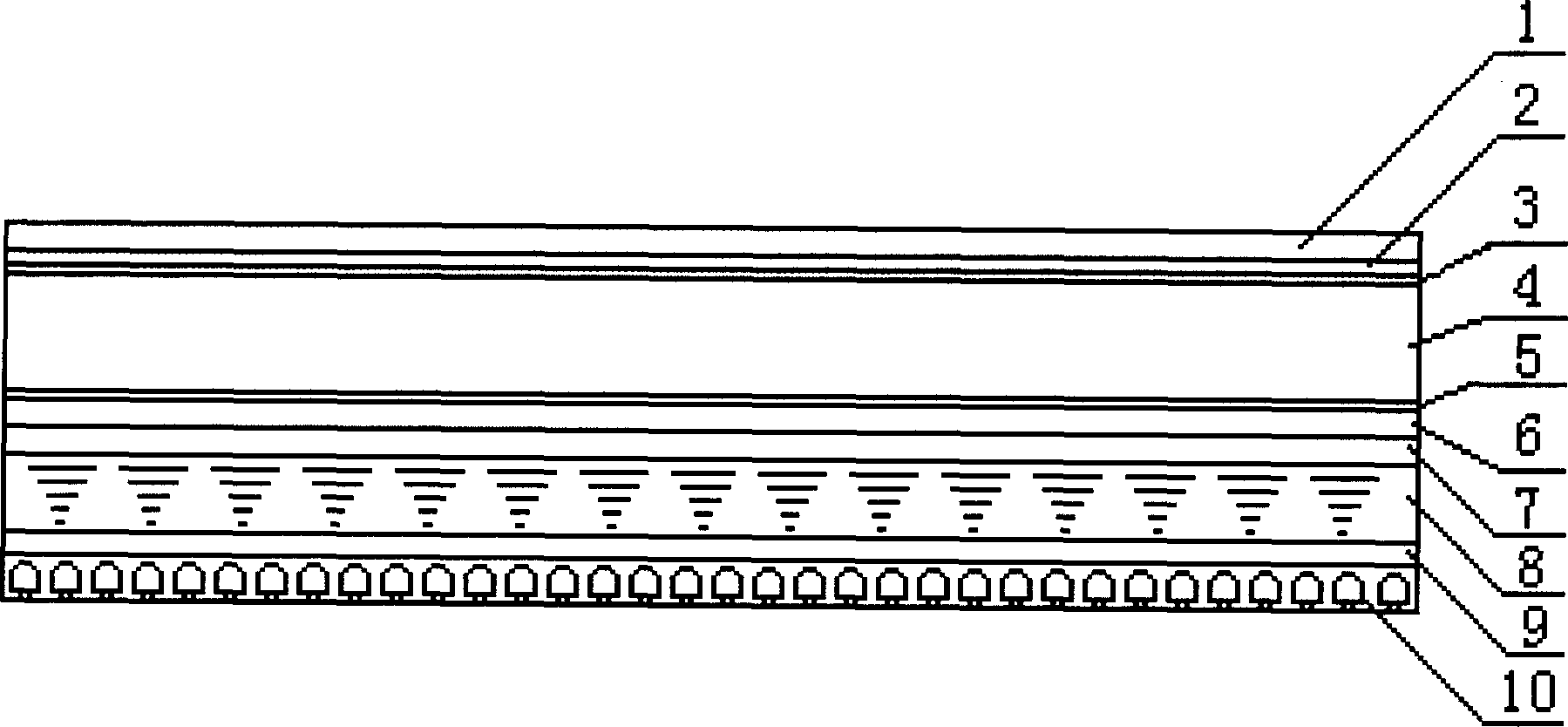
[0010] Referring to the accompanying drawings, the present invention includes a glass substrate 1 and a trichromatic phosphor array 2 arranged on the inner surface of the glass substrate 1 and an aluminum film 3 with a thickness of 1 to 1000 nanometers, and an ITO glass substrate 6 is arranged at the lower end of the glass substrate 1 A vacuum chamber 4 with a thickness of 1 to 6 mm is formed between the glass substrate 1 and the ITO glass substrate 6. The aluminum film 3 and the ITO glass substrate 6 are respectively connected to the positive and negative poles of DC high voltage, and the ITO glass substrate 6 is also evaporated. There is a photocathode array 5, and the positions of the photocathode array 5 and the trichromatic phosphor array 2 correspond one by one, and the lower side of the ITO glass substrate 6 is provided with an upper ITO glass substrate...


PUM

PropertyMeasurementUnit
thicknessaaaaaaaaaa
thicknessaaaaaaaaaa

Abstract

The invention relates to a separated field emission display device, which comprises a glass basic plate and the three primary colors fluorescent powder and aluminum film mounted on the glass basic plate. Wherein, there is a sealed vacuum chamber between the glass basic plate and the ITO glass basic plate; the aluminum film and the ITO glass basic plate are individually connected to the anode and cathode of direct current and high voltage; the ITO glass basic plate is plated with a photo-electric cathode array; the liquid crystal light valve is mainly formed by a upper ITO glass basic plate with directional layer, a liquid crystal layer and a lower ITO glass basic plate with directional layer, while the lower end of said liquid crystal light valve has a negative light source of light-emitting diode. The invention uses the electric beam to impact the fluorescent powder, the liquid crystal light valve and the negative light source, therefore, it has the energy saving, portable and better display properties of CRT and plane display, and compared to the surface conductive electric emitting display, it can avoid the preparation of nanometer slit to reduce the difficulty of technique and process.

Description

technical field [0001] The invention belongs to a field emission display device in the field of flat panel display, and in particular relates to a field emission display device with a discrete structure. Background technique [0002] With the improvement of people's visual requirements day by day, display technology has also developed rapidly, from cathode ray tube display (CRT), liquid crystal display (LCD), plasma display (PDP) to organic electroluminescent display (OLED) and field-induced Fluorescent display (FED), cathode ray tube display (CRT) has the disadvantages of large size, high power consumption and radiation, and gradually loses its dominance in the display field; and flat panel display technology is known as a rising technology and is the 21st As the mainstream of display technology development in the century, it has been widely valued by people. It must not only have perfect display quality, but also need more improvements in volume and energy saving. LCD, PD...

Claims


Application Information

Patent Timeline
Patent Type & Authority Applications(China)
IPC IPC(8): H01J31/12G02F1/13G09F9/00
Inventor 牟强李新贝张方辉马颖靳宝安张麦丽刘倩朱小娟
Owner SHAANXI UNIV OF SCI & TECH
Why Eureka
Try Eureka