Active matrix display device and data line switching circuit, switching section drive circuit, and scanning line drive circuit thereof

An active matrix and display device technology, applied in identification devices, nonlinear optics, static indicators, etc., can solve the problems of increased power consumption and large defects, and achieve the effect of improving long-term reliability and obtaining long-term reliability

Inactive Publication Date: 2006-08-16
SHARP KK
View PDF8 Cites 6 Cited by
  • Summary
  • Abstract
  • Description
  • Claims
  • Application Information

AI Technical Summary

Problems solved by technology

In particular, when the data line drive circuit 3 and the gate line drive circuit 200 are added to the liquid crystal panel 100, the switching unit drive circuit 102 is required, and the number of parts increases, causing a large disadvantage.
[0042] Moreover, in the above-

Method used


Image

  • Active matrix display device and data line switching circuit, switching section drive circuit, and scanning line drive circuit thereof
  • Active matrix display device and data line switching circuit, switching section drive circuit, and scanning line drive circuit thereof
  • Active matrix display device and data line switching circuit, switching section drive circuit, and scanning line drive circuit thereof

Examples


Embodiment 1

[0087] According to an embodiment of the present invention, based on Fig. 1~ Figure 7 It is explained as follows.

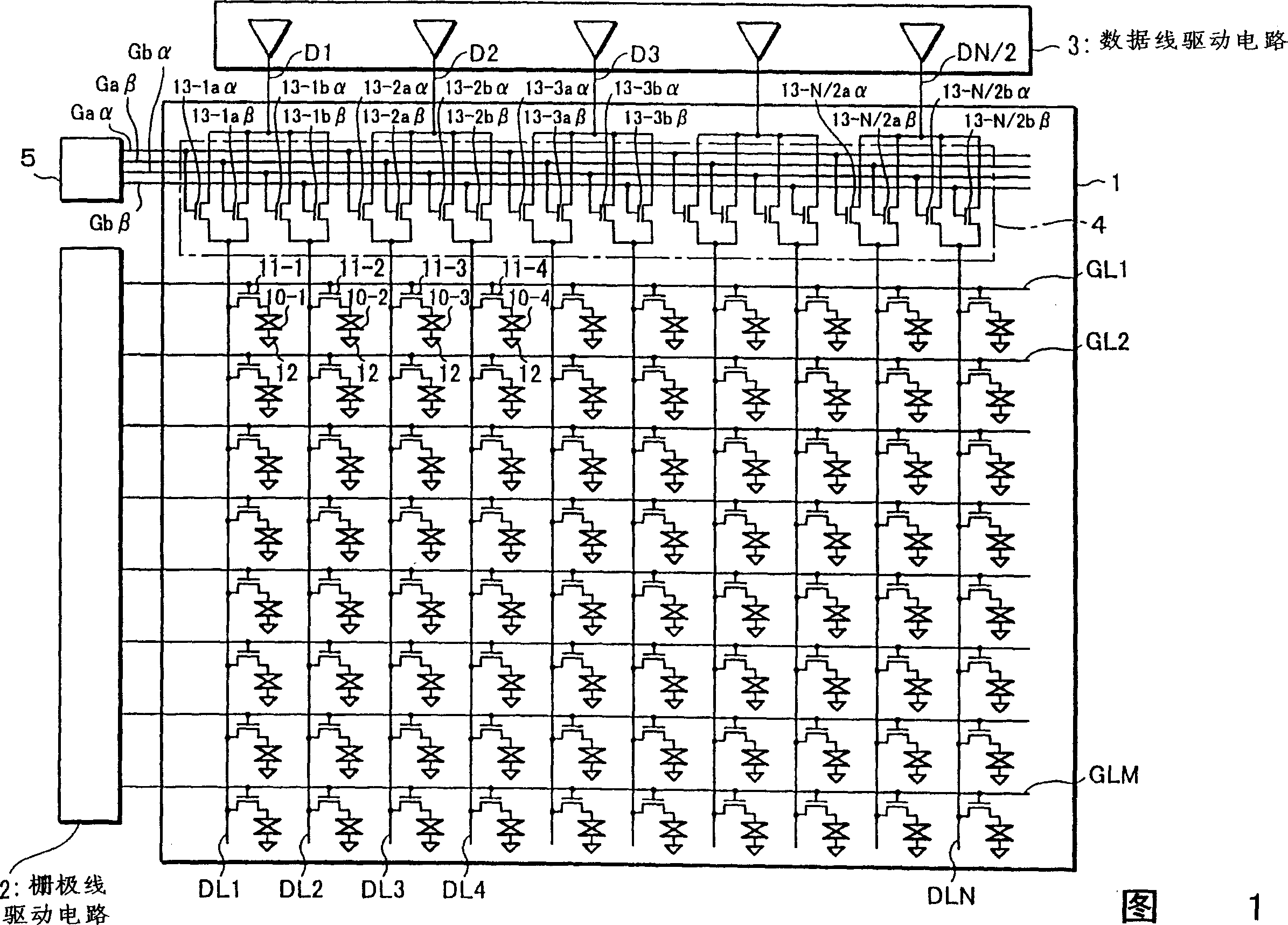
[0088] FIG. 1 is an equivalent circuit diagram of an active matrix liquid crystal display device according to an embodiment of the present invention. In this FIG. 1, the same components as those in the above-mentioned FIG. 20 showing the conventional example are denoted by the same symbols.

[0089] That is, in FIG. 1, 1 is a display panel (active matrix type display panel). Although not specifically shown in the figure, the liquid crystal panel 1 has a matrix substrate, a counter substrate, and a matrix substrate arranged in parallel and opposed to each other at a predetermined distance. Liquid crystals filled between the two substrates.

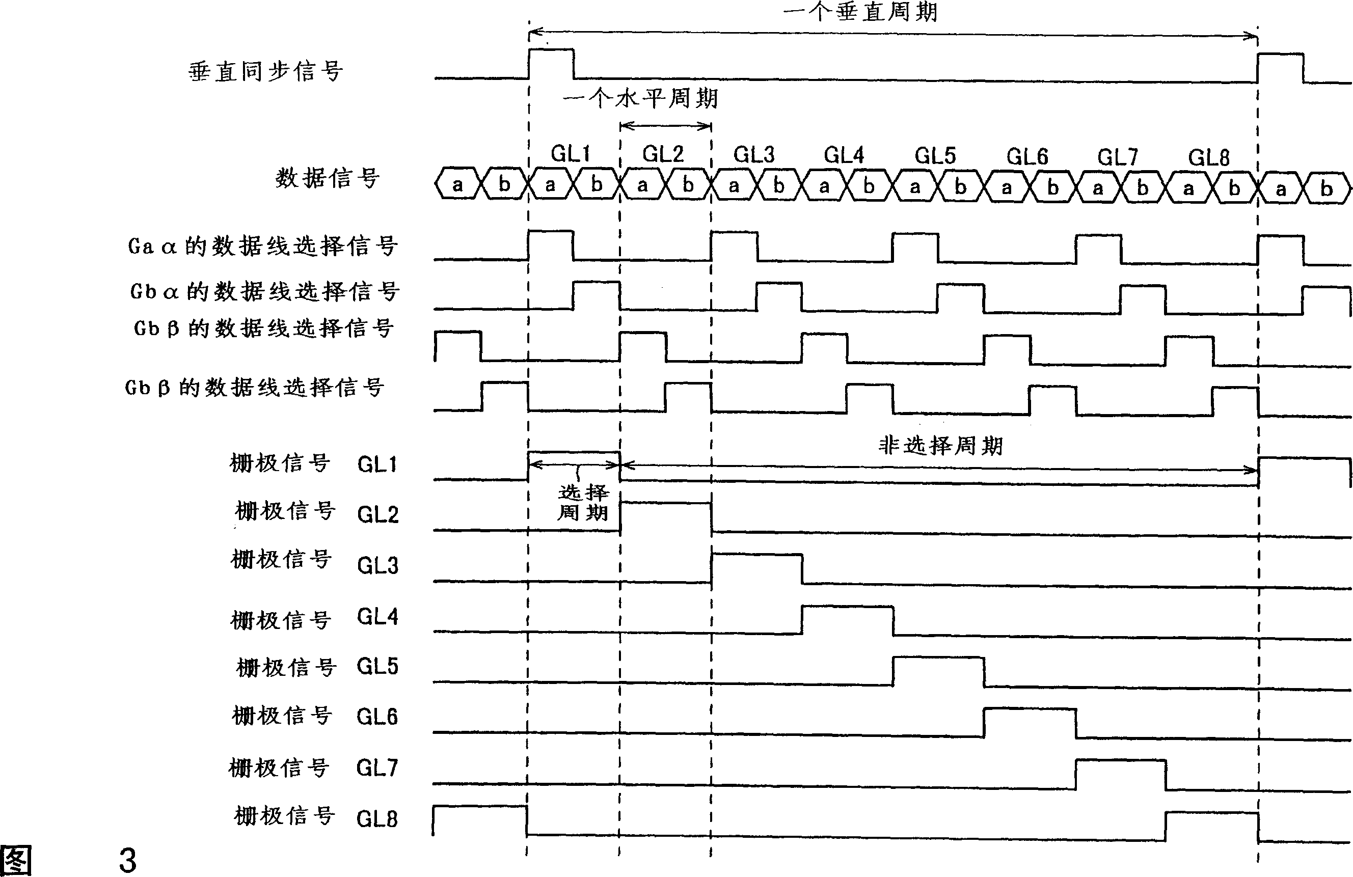
[0090] On the matrix substrate, a plurality of parallel data lines DL1 to DLN and a plurality of parallel gate lines (scanning lines) GL1 to GLM intersecting the data lines DL are provided. A gate signal having a turn-on v...

Embodiment 2

[0137] According to another embodiment of the present invention based on Fig. 8~ Figure 14 described as follows.

[0138] FIG. 8 is an equivalent circuit diagram of the configuration of the active matrix liquid crystal display device of this embodiment, and the same components as those shown in FIG. 20 showing the conventional example are denoted by the same symbols.

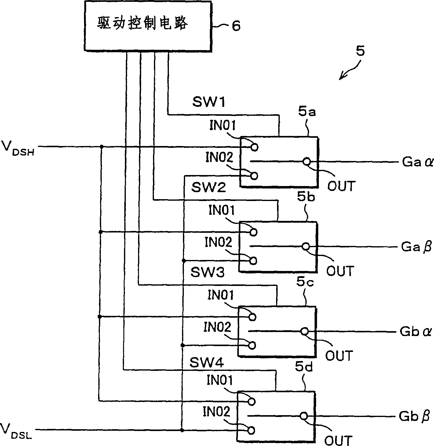
[0139] The first difference between the liquid crystal display device of this embodiment shown in FIG. 8 and the conventional liquid crystal display device shown in FIG. 20 is that in the liquid crystal display device of FIG. The switching part driving circuit 102 and the gate line driving circuit 200 for selecting the signal are provided independently. In the liquid crystal display device of FIG. In the line driving circuit 22 , a data line selection signal is output through the gate line driving circuit 22 . The details will be described below.

[0140] In FIG. 8, 100 is a display panel (active matrix type...

Embodiment 3

[0194] Here, an active matrix display device will be described in which the following two configurations are combined: the configuration described in Embodiment 1, in which the switching section of the data line switching circuit is formed by a plurality of switching elements; and Such a structure: as described in Embodiment 2, the switch unit drive circuit is built into the gate line drive circuit, and at the same time, various conduction voltages can be set in one gate line drive circuit, and the data of the switch unit can be driven. The turn-on voltage of the line selection signal and the turn-on voltage of the gate signal driving the pixel switch are different.

[0195] The following is based on Figure 15~ Figure 19 Another embodiment according to the present invention will be described. For convenience of description, components having the same functions as those used in Embodiments 1 and 2 are denoted by the same symbols, and descriptions thereof are omitted.

[0196...


PUM


Abstract

In an active matrix display device in which a data line switching circuit is provided and a plurality of data lines are grouped so as to be connected to one output of a data line drive circuit in order to reduce the number of the outputs of the data line drive circuit, switching elements constituting respective switching sections for selecting the data lines have a short life span so as to be unreliable in the long term. In contrast, a data line switching circuit in accordance with the present invention is provided with switching sections each composed of a plurality of switching elements connected in parallel to each other, so that the life span of the switching elements can be prolonged and the long-term reliability of the switching elements can be improved without obstructing the attempts such as narrowing a frame part and downsizing the whole device.

Description

[0001] This application was submitted by the applicant on September 30, 2002. The application number is "02149536.X", and the title of the invention is "Active matrix display device and its data line switching circuit, switch part driving circuit, scanning line driving A divisional application of the invention patent application for "circuit". Background of the invention [0002] The present invention relates to an active matrix type display device such as a TFT (Thin Film Transistor) type liquid crystal display device, and more specifically relates to a plurality of data lines to which a data signal as an image signal is applied are bundled together and one output of a data line driving circuit. The connected active matrix display device, and its data line switching circuit, switching unit driving circuit, scanning line driving circuit, etc. Background technique [0003] The liquid crystal display device has the advantages of being thinner than a CRT (Cathode Ray Tube) and ...

Claims


Application Information

Patent Timeline
IPC IPC(8): G09G3/36G09G3/20G02F1/133G02F1/1343G02F1/1368G09F9/30
Inventor 中野武俊西九保圭志川口登史
Owner SHARP KK
Why Eureka
Try Eureka