Optical glucose sensor chip
A sensor chip, glucose technology, applied in biochemical equipment and methods, analysis by chemical reaction of materials, material analysis by observing the impact on chemical indicators, etc. The effect of inhibiting dissolution and good diffusion
- Summary
- Abstract
- Description
- Claims
- Application Information
AI Technical Summary
Problems solved by technology
Method used
Image

Examples
Embodiment approach 1
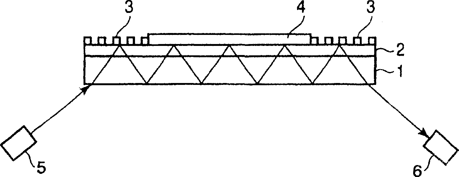
[0019] figure 1 It is a cross-sectional view showing the optical glucose sensor chip according to the first embodiment.
[0020] The glass substrate 1 has, for example, 3 nm or more on the main surface. Thickness of SiO 2 Surface 2. The optical components are made in the above SiO 2 The surfaces near the two edges of the surface layer 2 are respectively formed by injecting light into the substrate 1 or emitting light in the substrate 1, and a pair of gratings 3 are used. In addition, the optical components can also be replaced with prisms. These gratings 3 are made of SiO 2 The refractive index of the surface layer 2 is composed of, for example, titanium oxide. A protective film having a lower refractive index than the above-mentioned grating 3 is formed to cover the above-mentioned grating 3. The material of the protective film is made of, for example, a fluorine-based resin that does not react with the chemicals or samples used.
[0021] The SiO of the substrate 1 located betw...
Embodiment approach 2
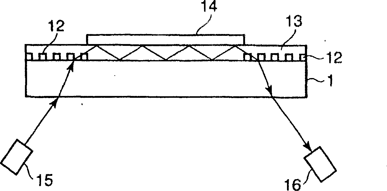
[0037] figure 2 It is a cross-sectional view showing the optical glucose sensor chip according to the second embodiment.
[0038] In order to inject and emit light on the glass substrate 11, a pair of gratings 12 as optical components are respectively formed near both edges of the main surface of the glass substrate 11. These gratings 12 are made of, for example, titanium oxide having a higher refractive index than the above-mentioned substrate 11. A light reflection path layer 13 made of a thermosetting or photocurable resin having a higher refractive index than the substrate 11 is formed on the main surface of the substrate 11 including the grating 12. The light reflection path layer 13 is formed so that its main surface is parallel to the main surface of the substrate 11 including the grating 12. A glucose sensor film 14 is formed on the light reflection path layer 13 corresponding to the part between the gratings 12. The glucose sensor film 14 contains an enzyme that oxidize...
Embodiment 1
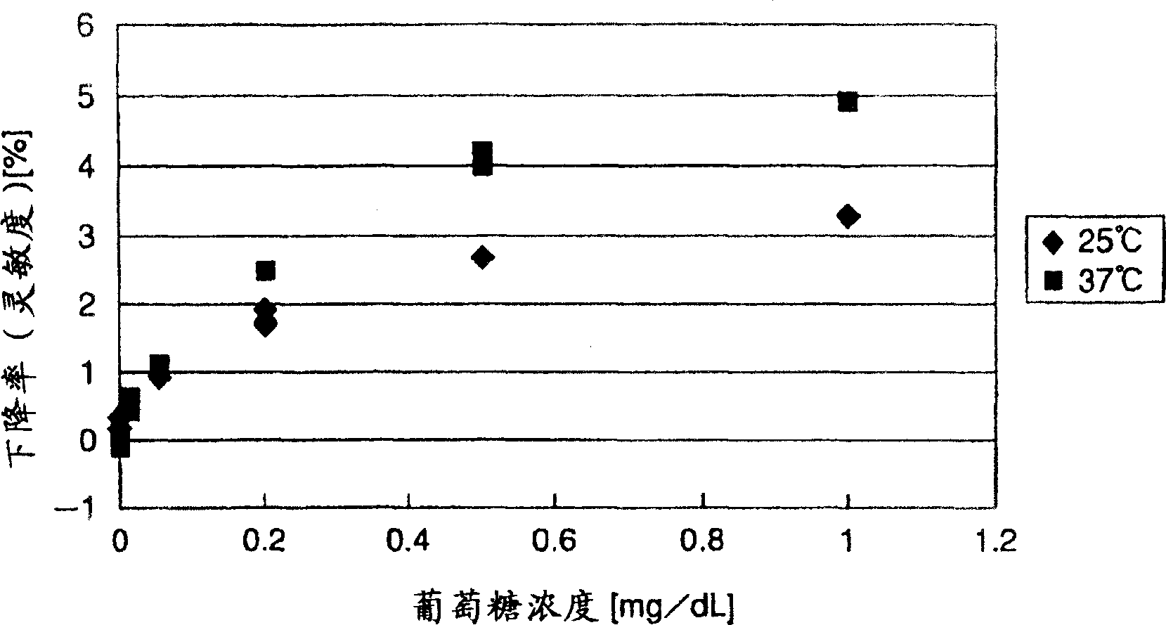
[0056] Mix 1436μL of isopropanol (IPA), 956μL of pure water, 210μL of 0.01 mol / L, pH 6.0 phosphate buffer, 60μL of 1% by volume polyethylene glycol (PEG) in isopropanol solution, 600μL of 1mg / ml of 3,3',5,5'-tetramethylbenzidine (TMBZ) in isopropanol, 640μL of 2% by weight carboxymethylcellulose (CMC) aqueous solution, 8μL of 1% by weight Linked polymer compound (2-methacryloyloxyethyl phosphorylcholine and butyl methacrylate copolymer) aqueous solution, 0.67 mg / mL peroxidase (POD) solution (dissolved in 0.01 mol / L Phosphate buffer (pH: 6.0)) and 5.33 mg / mL glucose oxidase (GOD) solution (dissolved in 0.01 mol / L phosphate buffer (pH: 6.0)), stir to prepare 4000 μL for generating glucose sensor Film coating liquid.
[0057] Next, prepare SiO with a thickness of 10nm on the main surface 2 The surface layer of the alkali-free glass substrate with a refractive index of 1.52, by sputtering, the SiO on the substrate 2 A titanium oxide film with a refractive index of 2.2 to 2.4 and a th...
PUM
| Property | Measurement | Unit |
|---|---|---|
| thickness | aaaaa | aaaaa |
| thickness | aaaaa | aaaaa |
| refractive index | aaaaa | aaaaa |
Abstract
Description
Claims
Application Information