Plasma processing apparatus and method

A plasma and processing device technology, applied in the field of ion plasma processing devices, can solve the problem that the time for applying DC voltage is not specified, etc.

Active Publication Date: 2006-10-04
TOKYO ELECTRON LTD
View PDF1 Cites 15 Cited by
  • Summary
  • Abstract
  • Description
  • Claims
  • Application Information

AI Technical Summary

Problems solved by technology

[0007] However, as in the above-mentioned Patent Document 1, in the case of applying a DC voltage, the application time has an influence ...

Method used


Image

  • Plasma processing apparatus and method
  • Plasma processing apparatus and method
  • Plasma processing apparatus and method

Examples


Embodiment Construction

[0070] Hereinafter, embodiments of the present invention will be specifically described with reference to the drawings.

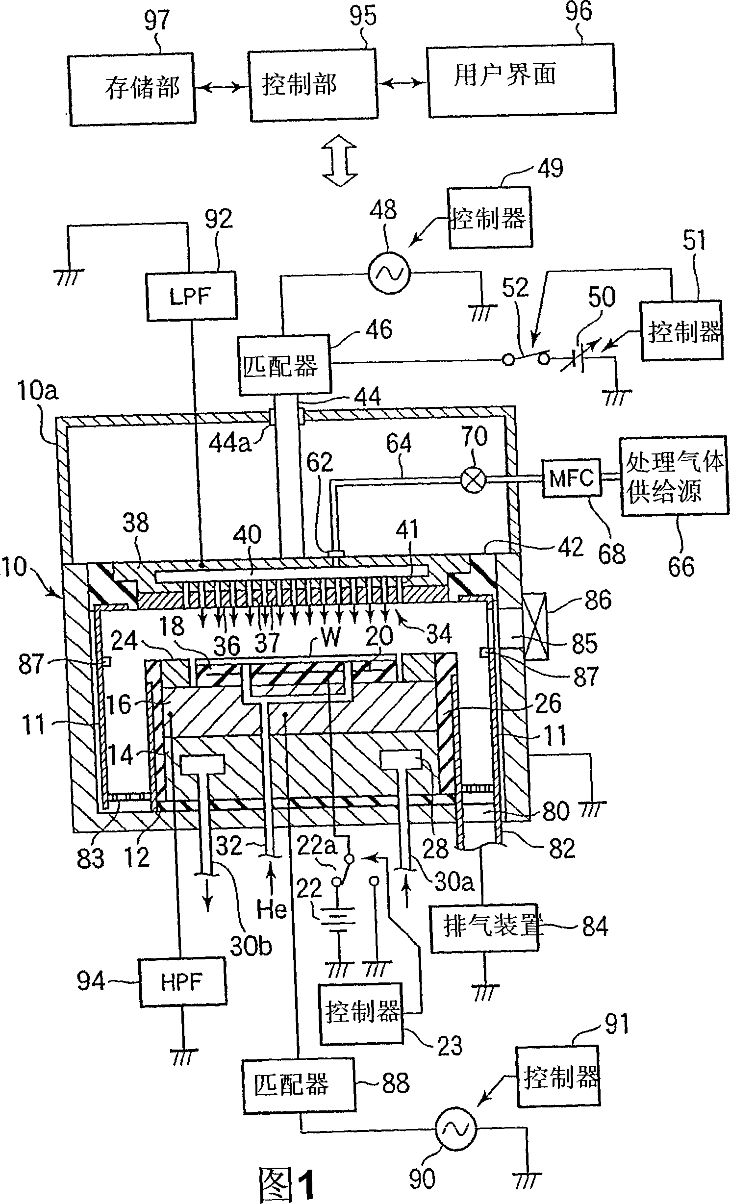
[0071] FIG. 1 is a schematic cross-sectional view of a plasma etching apparatus showing one embodiment of the plasma processing apparatus of the present invention.

[0072] This plasma etching apparatus is configured as a capacitive coupling type parallel plate plasma etching apparatus, and has, for example, a substantially cylindrical chamber (processing container) 10 made of anodized aluminum on the surface. The chamber 10 is securely grounded.

[0073] A cylindrical susceptor support 14 is disposed at the bottom of the chamber 10 via an insulating plate 12 made of ceramics or the like, and a susceptor 16 made of, for example, aluminum is provided on the susceptor support 14 .

[0074] On the susceptor 16 is provided an electrostatic chuck 18 holding a semiconductor wafer W as a substrate to be processed by static suction. A semiconductor wafer W is pla...


PUM


Abstract

The invention relates to a plasma processor and relative method with high frequency and direct current voltage, wherein in the plasma etching device that generating the plasma for processing gas between the upper and lower electrodes (34, 16) in chamber (10) and etching plasma chip (W), there is one high-frequency power supply (48) that supplies high-frequency electricity to the upper electrode (34) to form plasma; and a direct-current power (95) for supplying direct-current voltage to the upper electrode (34) and a controller for controlling the high-frequency power supply (48) and the direct-current power supply (50); with said controller (95), when the high-frequency power supply (18) powers, the voltage of variable direct-current power supply (50) is fixed.

Description

technical field [0001] The present invention relates to a plasma processing apparatus and a plasma processing method for performing plasma processing such as plasma etching on a substrate to be processed such as a semiconductor substrate. Background technique [0002] In the manufacturing process of semiconductor devices, in order to form circuits on a semiconductor wafer as a substrate to be processed, plasma etching treatment is used. Various apparatuses are used as apparatuses for performing plasma etching treatment, among which capacitive coupling type parallel plate plasma etching apparatuses are mainly used. [0003] Capacitance-combined parallel plate plasma etching device is to arrange a pair of parallel plate electrodes (upper and lower electrodes) in the chamber. A high-frequency electric field is formed, and the plasma of the process gas is formed by the high-frequency electric field, and the plasma etching process is performed on the semiconductor wafer. [000...

Claims


Application Information

Patent Timeline
IPC IPC(8): H05H1/46H01J37/32H01L21/3065
CPCH01J37/32174H01J37/32082H01J37/32091A47J27/022A47J27/14A47J36/36
Inventor 松本直树田中秀朗藤原尚舆水地盐小岩史明小林俊之仲山阳一中村博
Owner TOKYO ELECTRON LTD
Why Eureka
Try Eureka