Photonic crystal waveguide, homogeneous medium waveguide, and optical device

A photonic crystal waveguide and photonic crystal technology, applied in the direction of optical waveguide light guide, laser components, optics, etc., can solve the problems of arranging waveguides and design restrictions, and achieve the effect of small waveguide width and compact size

Inactive Publication Date: 2006-10-25
NIPPON SHEET GLASS CO LTD
View PDF11 Cites 22 Cited by
  • Summary
  • Abstract
  • Description
  • Claims
  • Application Information

AI Technical Summary

Problems solved by technology

Therefore, it is not possible to arrange waveguides at desired angles or various optical devices utilizing waveguides
This creates a design limitation

Method used


Image

  • Photonic crystal waveguide, homogeneous medium waveguide, and optical device
  • Photonic crystal waveguide, homogeneous medium waveguide, and optical device
  • Photonic crystal waveguide, homogeneous medium waveguide, and optical device

Examples


no. 1 example

[0373] When the above-mentioned one-dimensional photonic crystal is used in the design (for example, as Figure 20 In the case of the optical device shown), it is preferable to form the photonic crystal in the shape of a waveguide, because this facilitates the connection with the optical fiber, and facilitates the control of the above-mentioned characteristics ("extraordinarily large wavelength dispersion" and "group velocity anomaly") The electrodes are arranged.

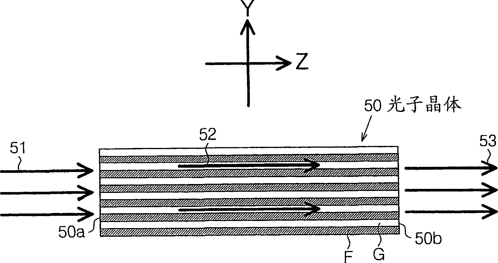
[0374] by using according to Figure 21 The photonic crystal waveguide 200 of the first embodiment shown is formed Figure 20 Optics shown. The photonic crystal waveguide 200 is formed in a waveguide shape on a suitable substrate 90 by using a one-dimensional photonic crystal as a core. For the photonic crystal forming the core of the photonic crystal waveguide 200 assigned with figure 1 The photonic crystal 50 has the same reference numerals, and its repeated description is omitted.

[0375] After converting ...

no. 2 example

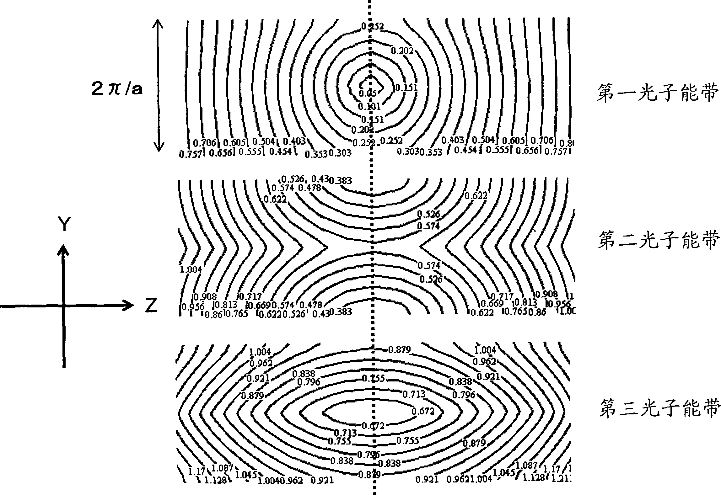
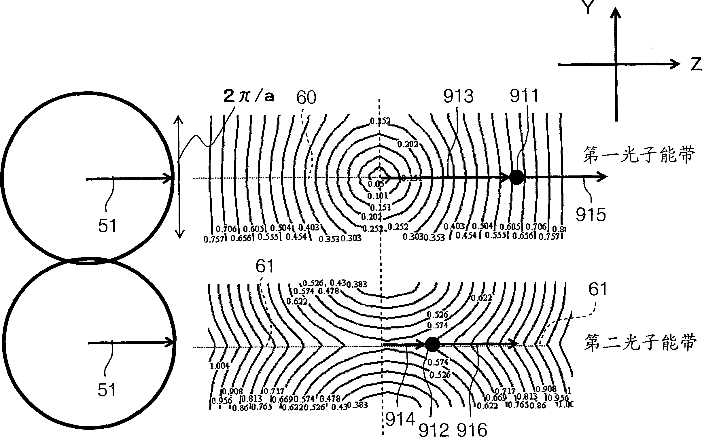
[0511] The following applies to the propagating light using the photon energy band at the center of the Brillouin zone, described in the first embodiment above and Figure 21 and 22 Confinement conditions in various directions of the illustrated photonic crystal waveguide 200 are described.

[0512] (Y direction mode)

[0513] Unlike the above propagation using "bands on the boundary of the Brillouin zone", in Figure 26 The second up-band propagating mode shown is the zeroth order mode with N=0. Do not use Figure 25 The "zero-order mode on the first energy band" is shown because its characteristics are close to those of ordinary plane waves.

[0514] (Single-mode condition in Y direction)

[0515] If the effective refractive index of the propagating mode is larger than that of the upper and lower cladding medium, confinement can be achieved due to the difference in refractive index. However, if the effective refractive index of the propagating mode is small, then in ...

no. 3 example

[0568] Next, a description will be given of a third embodiment in which the present invention is applied to a waveguide whose core is formed of a uniform material. Such as Figure 40 As shown, the homogeneous dielectric waveguide 300 according to this embodiment consists of a refractive index n with a finite thickness in one direction (Y direction) 0 It is formed of a uniform material, and includes a core 301 and a cladding 342 that propagate electromagnetic waves in a direction (XZ plane direction) perpendicular to the one direction.

[0569] The cladding 342 on the opposite surface perpendicular to the Y direction of the core 301 is formed of a one-dimensional photonic crystal having periodicity in the Y direction (the one direction). The cladding 342 is a confinement cladding for preventing electromagnetic waves propagating through the core 301 from leaking out from surfaces (top and bottom surfaces) perpendicular to the Y direction.

[0570] In such a configuration of th...


PUM

PropertyMeasurementUnit
angle of incidenceaaaaaaaaaa
lengthaaaaaaaaaa
widthaaaaaaaaaa

Abstract

A photonic crystal waveguide and a homogeneous medium waveguide that can be bent sharply and placed at a free angle and have a low propagation loss. The photonic crystal waveguide (200) has a core composed of a photonic crystal (50) having a periodicity in the Y-direction. An electromagnetic wave propagates along a band on the border of the Brillouin zone of the photonic band structure of the core. The side surface parallel to the Y-direction of the core is in contact with a homogeneous medium of refractive index ns. A condition lambda0 / ns>alambda / (lambda<2> / 4+a<2>)<0.5> is satisfied where lambda0 is the wavelength of the electromagnetic wave in the vacuum space, a is the period of the photonic crystal, and lambda is the period in an X-Z plane direction of the wave propagating through the core. This condition is essential to prevent light from leaking from the side surface of the photonic crystal waveguide (200). Therefore, satisfying the condition confines the wave propagating through the core inside the side surface when the propagation angle phi=0 DEG .

Description

technical field [0001] The present invention relates to a photonic crystal waveguide, and more particularly, to a photonic crystal waveguide employing a waveguide-shaped one-dimensional photonic crystal that propagates electromagnetic waves in a non-periodic direction, a homogeneous dielectric waveguide having a homogeneous dielectric core, and devices such as directional couplers and optical Optics for switching. Background technique [0002] Photonic devices with waveguides disposed on substrates are already in practical use. Recently, defect waveguides in two-dimensional photonic crystals (2D-PhC) have received much attention and considerable research and development work has been done on them. Specifically, two-dimensional photonic crystals are obtained by arranging regular holes in a thin film layer with a high refractive index (Si, etc.) to obtain a full photonic bandgap ( photonic bandgap) to form. When the 2D-PhC includes linear defects, the light entering the def...

Claims


Application Information

Patent Timeline
Patent Type & Authority Applications(China)
IPC IPC(8): G02B6/12G02F1/01G02F1/313G02F1/377H01S3/10
Inventor 橘高重雄大家和晃常友启司
Owner NIPPON SHEET GLASS CO LTD
Why Eureka
Try Eureka