Purification of hole transporting material by means of ultrafiltration and ion exchange chromatography
A hole-transporting material and hole-based technology, which is applied in the manufacture of electrical components, electrical solid-state devices, semiconductor/solid-state devices, etc., can solve problems such as the decline in luminous brightness of organic EL devices that have not yet been established, and achieve the purpose of suppressing the decline in luminous brightness and being easy to remove Effect
- Summary
- Abstract
- Description
- Claims
- Application Information
AI Technical Summary
Problems solved by technology
Method used
Image
Examples
no. 1 approach
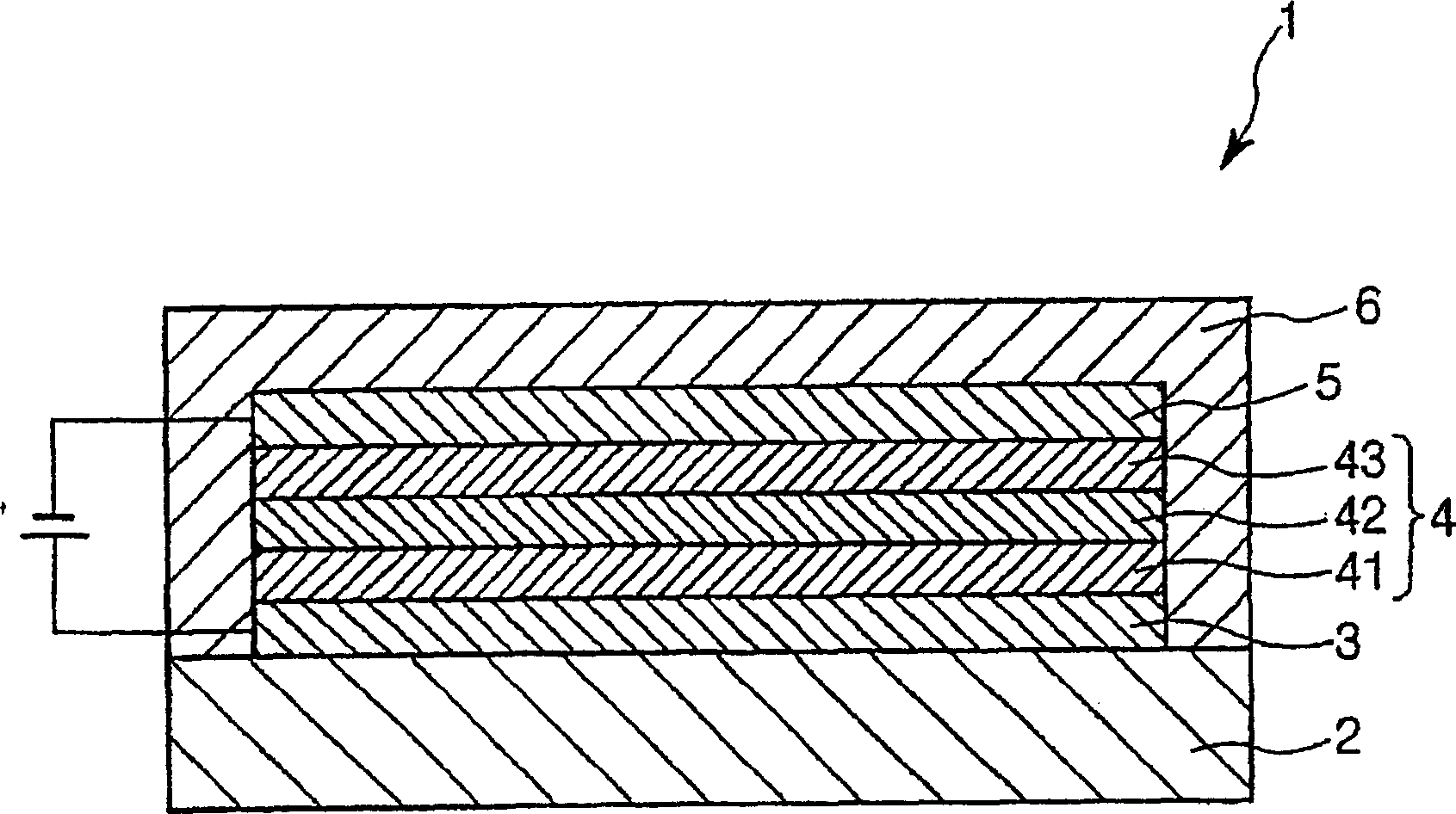
[0127] In order to suppress the decrease in the emission luminance of the organic EL device, the present inventors have conducted intensive investigations on all the layers constituting the organic EL device, and they have paid particular attention to the layer having the function of transporting holes.
[0128] As a result, the present inventors have found that the decrease in luminance of the organic EL device can be effectively reduced by reducing the amount of impurities contained in the layer capable of transporting holes, particularly nonionic impurities having a molecular weight of 5,000 or less (hereinafter, simply called "nonionic impurities") are suppressed by controlling the amount within a predetermined amount, thus completing the present invention. In the specification, this is described as the first embodiment.
[0129] As described above, in addition to the hole transport layer as a layer having a function of transporting holes, the hole injection layer and the ...
no. 2 approach
[0163] In addition to the above, the present inventors have also found that the decrease in the luminance of organic EL devices can be effectively reduced by adding anionic impurities, cationic impurities and nonionic impurities (hereinafter, simply referred to as "nonionic impurities" with a molecular weight of 5,000 or less) ") are suppressed by controlling the amount within a predetermined amount respectively, thus completing the present invention. In the specification, this is described as the second embodiment.
[0164] If the amount of impurities such as nonionic impurities, anionic impurities, and cationic impurities contained in the hole transport layer is large, a reaction occurs between the hole transport material and the impurities, or the hole transport material acts as a trigger due to the nonionic impurities Instead, structural changes (decomposition and the like, for example) occur, resulting in deterioration of the hole transport layer over time. In addition, ...
Embodiment 1A
[0227]
[0228] A 2.0 wt% aqueous solution of poly(3,4-ethylenedioxythiophene / styrenesulfonic acid) solution (which is a hole transport material and manufactured by Bayer Corp. under the product name "Baytron P") was first prepared as the Refined solution.
[0229] In the poly(3,4-ethylenedioxythiophene / styrenesulfonic acid) used, the weight ratio of 3,4-ethylenedioxythiophene to styrenesulfonic acid was 1:2.
[0230] Then, the solution used for purification was diluted 10 times with ultrapure water to prepare a solution.
[0231] Then, the solution thus prepared for purification was passed through an ultrafiltration unit (which is a stirring-type unit, type 8200 manufactured by Millipore Ltd., and its ultrafiltration membrane has a molecular weight cutoff of 3,000) and then it was concentrated until its The amount becomes the same as that of the solution used for purification before being diluted to remove nonionic impurities having a molecular weight cutoff of 3,000 or le...
PUM
 Abstract
Description
Claims
Application Information
